Dear readers, the core chips in your daily smartphones, computers, and AI devices are “refined” in wafer fabs (Fab)! This detailed guide on the Fab process breaks down the complete link from wafers to chips, the 10 core technologies, and departmental responsibilities, making it easy for both semiconductor newcomers and tech enthusiasts to understand the “black magic” of chip manufacturing.
1. Understanding the IC Industry Chain and the Core Position of Fab
Chip manufacturing cannot be accomplished by a single company; the entire industry chain is divided into three steps:
- IC Design (Fabless): For example, Qualcomm and Huawei HiSilicon, responsible for drawing the “circuit diagram” of the chip;
- Wafer Manufacturing (Fab): For example, TSMC and SMIC, which “print” the circuit diagram onto the wafer to create the chip die;
- Packaging and Testing (OSAT): For example, JCET and Amkor, which package and protect the die, testing performance before shipment.
Key Point: Fab is the “core factory” of the industry chain, equivalent to the “delivery room” for chips, starting from 8-inch/12-inch wafers and going through hundreds of processes to finally become densely packed chip dies.
2. Core Processes: The Two Major Stages of Fab Manufacturing (Front-End + Back-End)
Chip manufacturing is divided into “Front-End (FEOL) + Back-End (BEOL)”, with clear divisions of labor, both of which are essential:

In simple terms: Front-End = building the “house” (transistors), Back-End = paving the “road” (metal interconnections), finally connecting the house to create a functional chip.
3. Essential Knowledge: Analysis of the 10 Core Technologies in Fab
These 10 technologies are the “soul” of chip manufacturing, and each step must be executed flawlessly. Key points are summarized in the table:
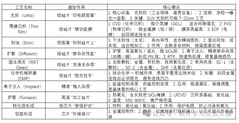
Key Point: Photolithography is the “most critical process”, directly determining the precision of the chip; the more advanced the photolithography machine (such as EUV), the finer the process nodes (such as 5nm, 3nm) that can be achieved.
4. Fab Department Responsibilities: Who is Responsible for Chip Manufacturing?
A Fab has multiple departments working together, each with its own responsibilities; none can be missing:
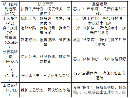
5. Key Trends: The Three Core Directions of Fab Manufacturing
- Process nodes are becoming finer: From 28nm→14nm→7nm→3nm, relying on more advanced EUV lithography machines and fine processes;
- Larger wafer sizes are better: From 8 inches→12 inches→future 450mm, allowing more chips to be produced from a single wafer, reducing costs;
- Higher integration levels: 3D packaging and heterogeneous integration enhance chip performance and reduce power consumption, adapting to AI and 5G demands.
Interactive Time
Dear readers, after reading this, do you have a new understanding of chip manufacturing? Which process (such as lithography or etching) would you like to learn more about? Or do you have questions about the Fab departmental responsibilities? Leave your questions in the comments!
#SemiconductorManufacturing #FabProcess #ChipManufacturing #WaferFab #SemiconductorKnowledge #ChipIndustryChain #LithographyProcess #SemiconductorDepartmentResponsibilities