The purpose of this article is to introduce the theory and knowledge related to high-speed ADCs, detailing sampling theory, data sheet specifications, ADC selection criteria and evaluation methods, clock jitter, and other general system-level considerations. Additionally, some users hope to further enhance the performance of ADCs through techniques such as interleaving, averaging, or dithering.
1. Introduction
The basic ADC block diagram and terminology are shown in the figure below: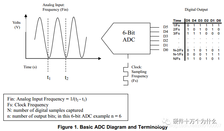
With the improvement in digital signal processing technology and the operational speed of digital circuits, as well as the increasing demands for system sensitivity, high-speed and high-precision specifications for ADCs (Analog to Digital Converters) and DACs (Digital to Analog Converters) have also become more stringent. For example, in radar and satellite communications, the required signal bandwidth has reached over 2 GHz, and the next generation of 5G mobile communication technology may also utilize signal bandwidths exceeding 2 GHz when operating in the millimeter wave frequency band. Although some scenarios (such as linear frequency modulation radar) may use frequency band stitching to achieve high bandwidth, this method is rather complex and imposes many restrictions on the transmission of communication or other complex modulated signals.
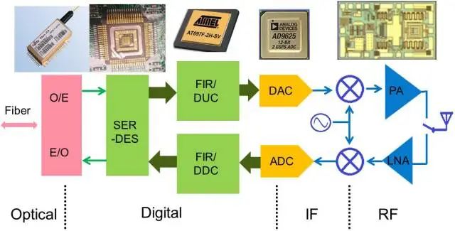
According to the Nyquist sampling theorem, the sampling rate must be at least twice the signal bandwidth. Furthermore, to support flexible standards, phased array, or large-scale MIMO beamforming, modern transceiver modules increasingly adopt direct sampling of digital intermediate frequency, which further raises the performance requirements for high-speed ADC/DAC chips. The following diagram illustrates the structure of a typical all-digital radar transceiver module.

Applications of High-Speed ADCs/DACs in Modern All-Digital Radars
It can be seen that ADC/DAC chips are the boundary between the analog and digital domains. Once the signal is converted to the digital domain, all signals can be processed and compensated through software algorithms, and this processing typically does not introduce additional noise or signal distortion. Therefore, moving the ADC/DAC chips forward to achieve all-digital processing is the trend in the development of modern communication and radar technologies.
In the course of all-digital development, ADC/DAC chips are required to sample or output signals at increasingly higher frequencies and bandwidths. However, the noise and signal distortion caused during the conversion from analog to digital or digital to analog are often challenging to compensate for and can significantly impact system performance. Therefore, the performance of high-speed ADC/DAC chips when sampling or generating high-frequency signals is crucial for system specifications.
Currently, in many specialized fields, the sampling rates of ADCs/DACs can reach very high levels. For example, Fujitsu can provide IP cores with sampling rates of 110G~130GHz, Keysight uses a 40GHz sampling rate, 10bit ADC chip in high-precision oscilloscopes, and Keysight also uses a 92GHz sampling rate, 8bit DAC chip in high-bandwidth arbitrary waveform generators. These specialized chips are typically used in special applications, such as optical communications or high-end instruments, and are relatively difficult to obtain independently.
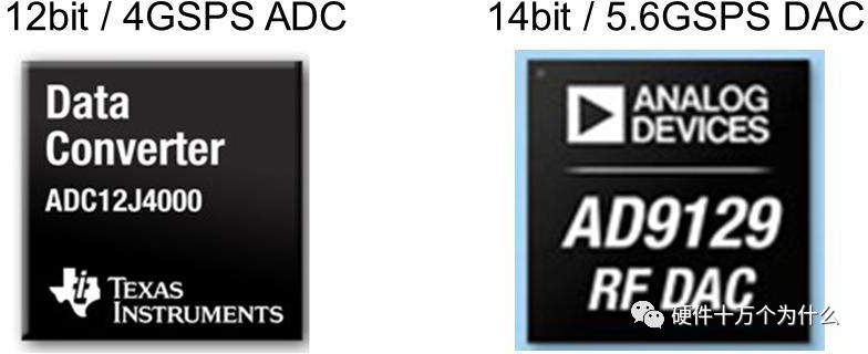
In the commercial sector, many ADC/DAC chips have also achieved sampling rates exceeding GHz, such as TI’s ADC 12J4000 with a 4 GHz sampling rate and 12bit resolution; and ADI’s AD9129 with a 5.6 GHz sampling rate and 14bit resolution. This requires ADCs to have relatively high sampling rates to capture high-bandwidth input signals, while also needing a relatively high number of bits to resolve subtle changes.
As the sampling rates of ADCs/DACs increase, the digital side interface technology of high-speed ADCs/DACs is also undergoing significant changes.
Low-speed serial interfaces: Many low-speed ADC/DAC chips use low-speed serial buses such as I2C or SPI to multiplex multiple parallel digital signals onto a few serial lines for transmission. Since the transmission speed of I2C or SPI buses is mostly below 10Mbps, such interfaces are mainly suitable for ADC/DAC chips with sampling rates below MHz.
Parallel LVCMOS or LVDS interfaces: For chips with sampling rates of several MHz or even hundreds of MHz, due to the high data rate after signal multiplexing, parallel data transmission methods are generally adopted, meaning that each bit resolution corresponds to one data line (for example, a 14-bit ADC chip uses 14 data lines), and these data lines share one clock line for signal transmission. The advantage of this method is that the interface timing is relatively simple, but since each bit resolution occupies one data line, it consumes more chip pins.
JESD204B serial interface: For higher-speed ADC/DAC chips, due to the higher sampling clock frequency and smaller timing margin, routing with parallel LVCMOS or LVDS interfaces becomes very challenging and occupies a large routing space. To address this issue, more advanced and miniaturized ADC/DAC chips have started to adopt the serial JESD204B interface. The JESD204B interface combines multiple bits of data to be transmitted onto one or several pairs of differential lines while using the currently mature SerDes (serial-deserialization) technology to transmit signals in data frame format, with each pair of differential lines having independent 8b/10b encoding and clock recovery circuits. This method has several advantages: first, the data transmission rate is higher, with each pair of differential lines achieving a maximum signal transmission of 12.5 Gbps according to current standards, allowing high-speed data transmission with fewer line pairs; second, the pairs of lines no longer share the sampling clock, greatly relaxing the requirement for equal length between the pairs of differential lines; leveraging modern SerDes chips’ pre-emphasis and equalization technology can achieve longer distance signal transmission, even allowing direct modulation of data onto light for long-distance transmission; and it allows for flexible chip replacement, as by adjusting the frame format in the JESD204B interface, the same set of digital interfaces can support different sampling rates or resolutions of ADC chips, facilitating system updates and upgrades.
Main Static Indicators:
Differential Non-Linearity (DNL)
Integral Non-Linearity (INL)
Offset Error
Main Dynamic Indicators:
Total harmonic distortion (THD)
Signal-to-noise plus distortion (SINAD)
Effective Number of Bits (ENOB)
Signal-to-noise ratio (SNR)
Spurious free dynamic range (SFDR)
The static indicators are obtained by performing histogram statistics on the amplitude distribution of the sampled data from the sine wave, which are then indirectly calculated. As shown in the figure below, the amplitude distribution of an ideal sine wave should resemble the shape on the left, but due to the influence of non-linearity and other factors, the distribution may change to the shape on the right. By comparing the actual histogram with the ideal histogram, the static parameter indicators can be derived.
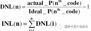
The following are the calculation formulas for DNL and INL:
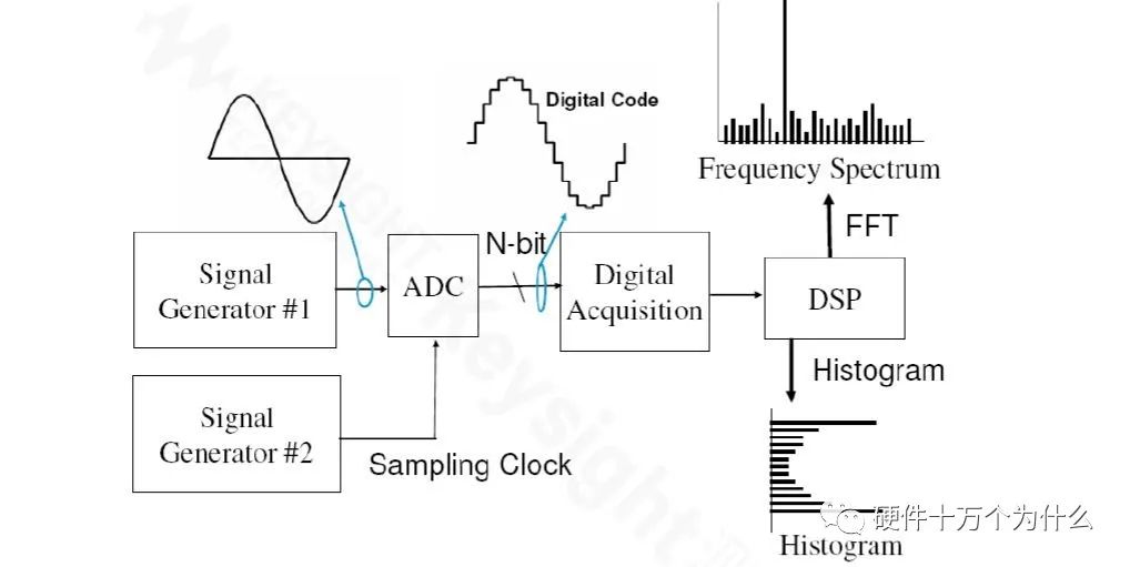
Dynamic indicators are derived from performing FFT spectral analysis on the sampled data from the sine wave, and then calculating the distortion in the frequency domain indirectly. An ideal sine wave sampled by A/D may take on the shape shown in the figure below after post-frequency spectral analysis. In addition to the main signal, due to the noise and distortion of the ADC chip, many additional noise, harmonics, and spurious components appear in the spectrum. By calculating these components, the dynamic parameters of the ADC can be obtained.
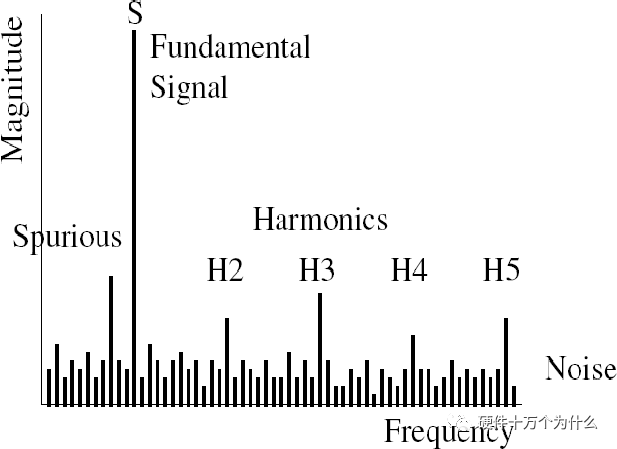
Testing Dynamic Parameters Through FFT Spectral Analysis
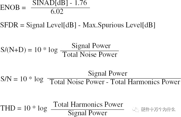
The following are the calculation formulas for dynamic parameters:
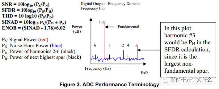
2. Spectrum Performance Terminology
SNR: Signal-to-noise ratio refers to the ratio of base frequency power to the noise floor power after removing DC and the first five harmonics; some data sheets may require removing the first nine harmonics. The base frequency is also called the signal or carrier. The unit of SNR is dBc (when using the absolute value of the base frequency as a reference); or dBFS.
SFDR: Spurious-free dynamic range. SFDR is the ratio of base frequency power to the highest spurious power.
THD: Total harmonic distortion. THD is the ratio of base frequency power to the power of the first five harmonics. THD is typically measured in dBc. Similar to SNR, some data sheets may use the first nine harmonics to calculate THD.
SINAD: Signal noise and distortion. The unit of SINAD can be dBc or dBFS.
Ideal SNR = 6.02*n + 1.76, where n is ENOB; for an ideal ADC, since there are no harmonics, its SINAD = SNR. For example, if a designer needs an ADC with a SINAD of 75dB, then ENOB = (75 – 1.76) / 6.02 = 12.2 bits, which means they need to select at least a 14-bit or even a 16-bit ADC to meet the requirement.
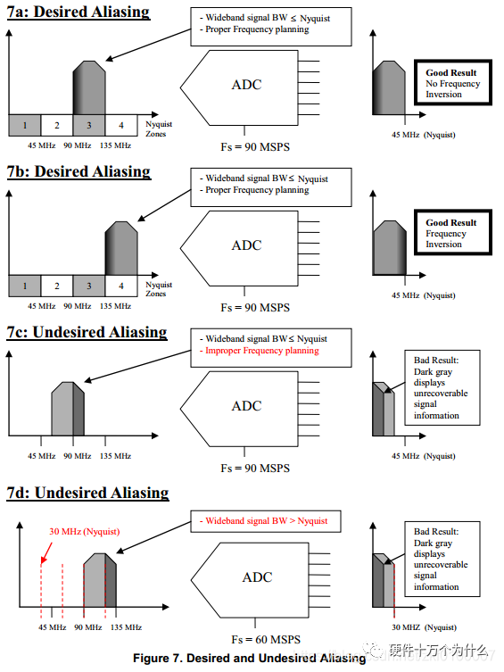
3. Nyquist, Aliasing, Undersampling, Oversampling, and Bandwidth
According to the Nyquist sampling theorem, the sampling clock frequency must be at least twice the frequency of the input analog signal.
4. ADC Pin Interfaces
Generally, ADCs include the following six types of interfaces:
-
Analog Input
-
Reference/Common Mode
-
Clock Input
-
Digital Output
-
Power Supply
-
GND
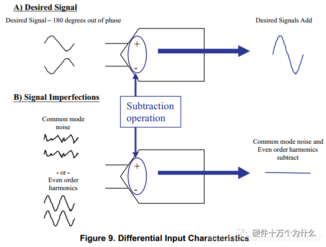
4.1 Analog Input High-speed ADCs typically use differential inputs, where the input signals are 180 degrees out of phase, allowing the signals to be superimposed. Compared to single-ended inputs, differential signals improve the noise characteristics of the ADC by eliminating common-mode noise. Additionally, differential signals reduce even-order harmonics due to the 180-degree phase shift of the signal, resulting in phase shifts of 2×180, 4×180, and 6×180 degrees for even-order harmonics, as shown in the figure below.
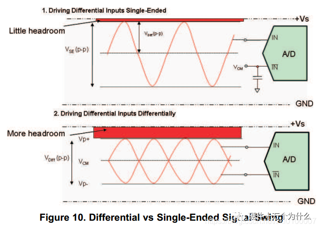
Compared to single-ended signals, the amplitude of the differential signal is only half that of the equivalent single-ended signal, resulting in better harmonic performance. Small signals allow the ADC to have a wider margin. Generally, more margin enables the ADC to operate in the linear region, reducing the nonlinear effects that produce harmonics. As shown in the figure below:

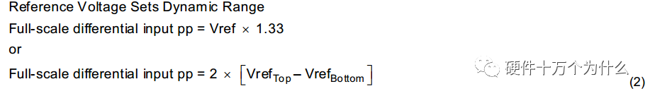
The reference voltage can be generated internally by the ADC or provided externally. To achieve the performance specified in the data sheet, the correct reference voltage must be supplied. For external references, efforts should be made to minimize the DC noise of the external reference voltage. Noise on the reference voltage directly affects the SNR of the ADC.
In Figure 11, the common-mode voltage VCM refers to the DC level of the differential analog input signal. VCM is used to bias the differential input signal between the power supply and GND.
There are several applications for VCM:
-
Some ADCs have VCM pins that output the internally generated VCM. -
Some ADCs set VREF equal to the level of VCM, thus allowing VREF to generate VCM. -
Designers can choose to provide VCM externally.
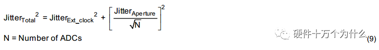
High-speed ADCs typically use differential clock inputs. Clock jitter and slope are important factors affecting the SNR of the ADC. The impact of clock jitter on SNR is illustrated as follows:

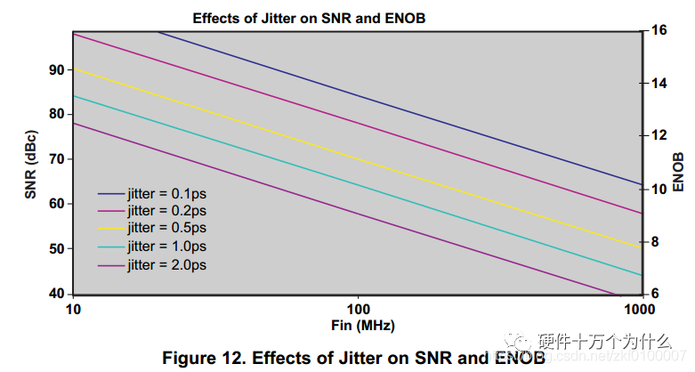
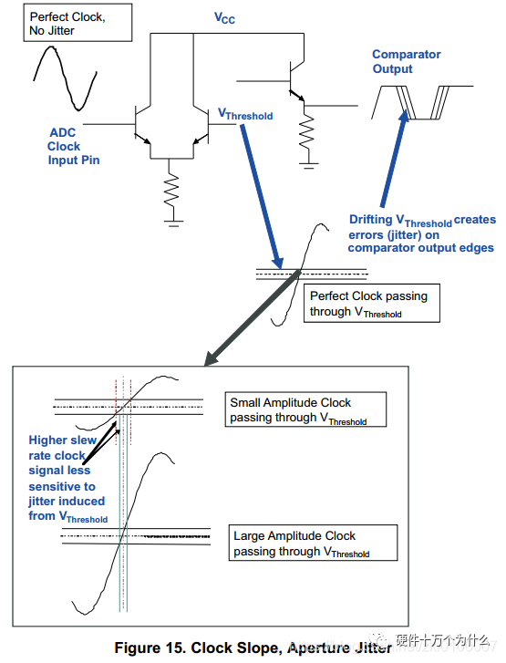
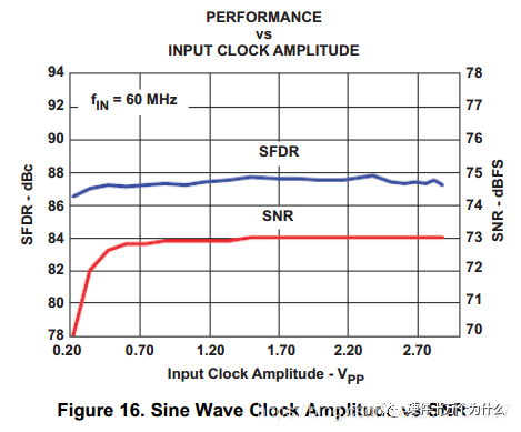
As can be seen, for an ideal ADC, the clock frequency does not affect the SNR. If clock jitter is not considered, the clock frequency may reach the design limits of the ADC (such as setup, hold, or analog setup times), ultimately leading to a decrease in SNR. With jitter remaining constant, SNR decreases as the input signal frequency increases. As shown in the figures, when specifying clock jitter, SNR decreases with increasing signal frequency. High-frequency analog input signals have a significant error due to clock jitter. If random noise is present on the clock signal, it will manifest in the spectrum. If there is a deterministic error signal on the clock signal, this signal will mix with the ADC’s input signal, appearing as spurious in the spectrum. Designers must consider two important factors regarding clock jitter: the aperture delay of the ADC and the jitter of the external input clock. The combined jitter from these two factors affects the sampling error of the ADC. Design example: The design requirements are as follows: SNR = 75dB, FIN = 75MHz, the selected ADC’s aperture jitter = 80fs. To meet the customer’s SNR requirement, what is the maximum allowable external clock jitter? A: Solve the jitter using formula 3. B: Solve the external clock jitter using formula 4. Therefore, the external input clock jitter must be less than 397fs. The diagram below illustrates the situation where slow clock edges lead to larger aperture jitter. For a sine clock, increasing the clock amplitude can improve aperture jitter, thereby enhancing the SNR of the ADC.
So the question arises, if we focus on the clock’s rising edge, why not directly provide the ADC with a square wave clock signal? The answer is: a square wave clock is indeed a feasible clock choice for the ADC. However, designers must make a series of trade-offs between sine and square waves.
One is the trade-off between low-jitter square wave clocks and clock frequency range. For most applications, improving the close-in phase noise (jitter) of the ADC clock can be achieved through narrowband SAW or crystal filters. After filtering, the clock becomes a low-jitter sine clock that can be directly supplied to the ADC. The limitation of this method is that the clock frequency range is constrained by the filter bandwidth. Some companies offer clock jitter cleanup and distribution chips that exhibit good phase noise performance, square wave output, and a wide frequency range, with phase noise characteristics sufficient to meet system requirements without the need for additional filters.
The second is the trade-off in signal integrity between square wave clocks and sine clocks. Compared to sine signals, square wave signals contain rich harmonics and high-frequency components. Due to signal reflections and interference with other signals, high-frequency components can pose significant challenges for circuit design. Regardless of the clock signal used, careful consideration must be given to circuit design to meet the jitter requirements of the ADC.
The experimental evaluation of ADCs mainly includes both software and hardware aspects.
The software methods for ADC experimental evaluation primarily involve FFT. Due to its speed and accuracy, FFT is an excellent evaluation tool for transforming time domain to frequency domain.
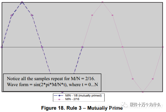
To implement FFT, it is essential to understand concepts such as consistency, windowing, and spectral leakage.
The diagram below illustrates windowing and spectral leakage. Improper window selection can lead to spectral leakage.
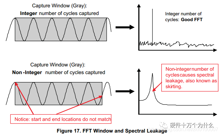
Some designers require non-integer cycles. In these special cases, due to spectral leakage, FFT cannot be used; instead, Blackman windows or Fourier analysis can be utilized. This method allows for the collection of non-integer cycle signals but requires more computation time and introduces slight errors in noise floor calculation and frequency response.
FFT consistency is defined as follows:
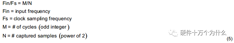
Rule 4: The resolution of FIN and FS must exceed the minimum resolution requirements of the input source. For example, if the minimum resolution for the analog input and clock source is 10Hz, they cannot be set to resolutions below 10Hz. When performing FFT, if the frequency resolution is less than the input source resolution, non-integer cycles will be collected, leading to spectral leakage.
Design Example: The requirements are as follows: Fin = 70MHz, Fs = 125Msps, resolution is 1Hz. Solve for M, N, Fin, and Fs. 1) Take N = 8192, M = NFin/Fs = 4587.52, round M = 4587.2) Recalculate Fs based on N (ensure the resolution is 1Hz) X = Fs/N = 125M/8192 = 15258.789, round to Xnew = 15258. New Fs = XnewN = 152588192 = 124.993536Msps 3) Calculate the new Fin Fin = FsM/N = 124.993536Msps*4587/8192 = 69.9988446MHz.
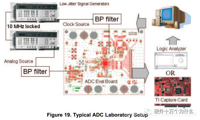
A typical ADC experimental setup is shown in the figure below:
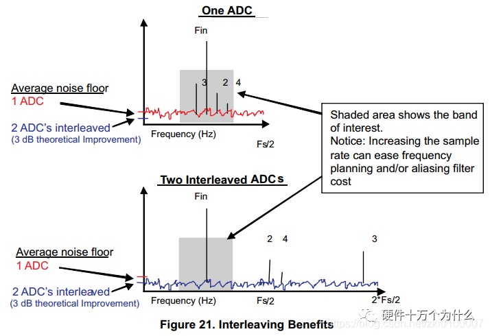
5. Interleaved Sampling
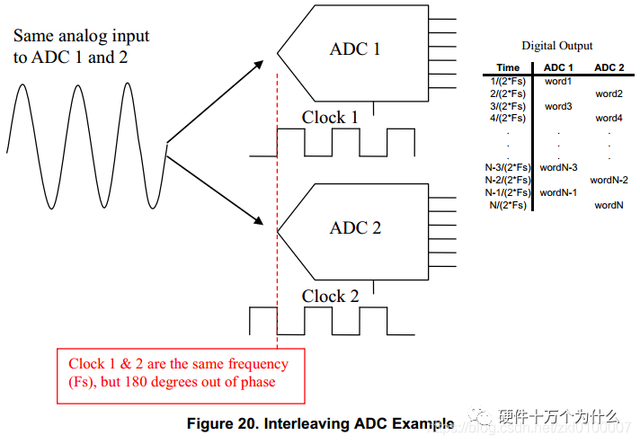
Two ADCs are connected in parallel to the analog input, with their sampling clocks offset by 180 degrees, effectively doubling the sampling speed. Doubling the sampling speed has two benefits: firstly, it increases the sampling signal bandwidth; secondly, interleaved sampling extends the noise floor over a wider bandwidth, potentially lowering the noise floor by 3dB, as illustrated in the figure below:
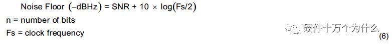
The noise floor calculation formula for a single ADC is as follows:
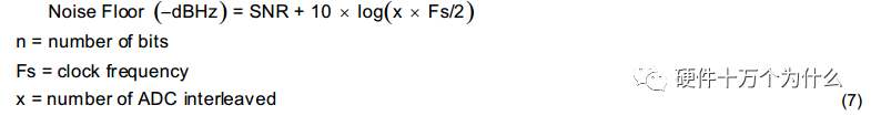
When multiple ADCs are interleaved, the noise floor calculation formula is as follows:
Interleaving two or more ADCs also introduces additional design challenges. Differences in DC offset between the ADCs can generate spectral components at specific locations. Differences in gain, INL, and clock phase errors between the ADCs can produce spectral components at the mixing points of the clock and analog input.
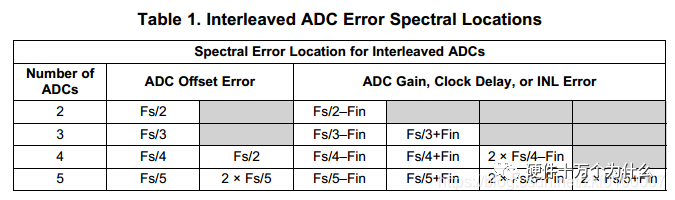
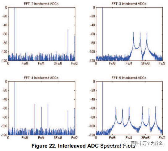
As seen in the figure, although the ADC errors are minimal, they can still cause significant spurious responses. Designers need to implement corresponding analog or digital filters with temperature compensation to filter out these spurious components.
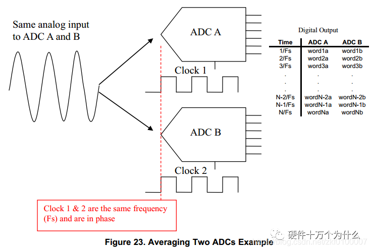
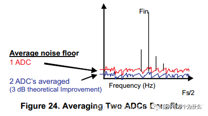
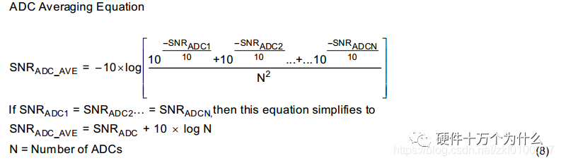
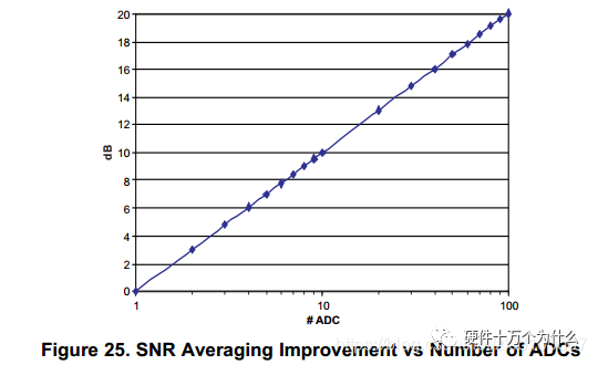
6. Averaging of ADCs
Another method to improve the SNR performance of single-chip ADCs is to average two or more ADCs. Averaging two ADCs can improve the SNR by 3dB.
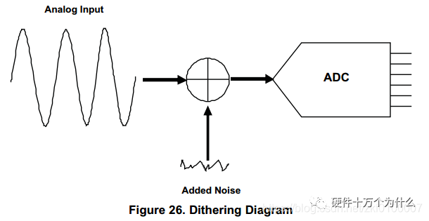
7. Jitter (Dithering)
ADCs exhibit deterministic and systematic errors, which are repeatable. Theoretically, these errors can be minimized by adding a low-level random noise. The process of adding low-level random noise to improve ADC distortion is called dithering.
-
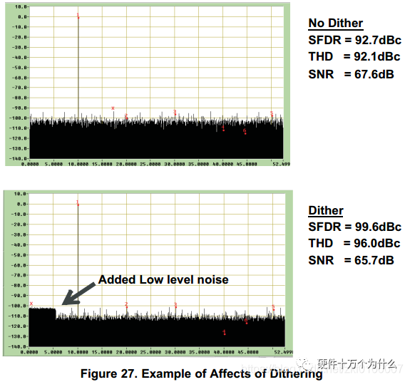
Dithering can lower the level of harmonics, but it may have a negative impact by increasing the noise floor. -
Improvements in harmonic performance depend on the type and amplitude of the signal; in some cases, there may even be no improvement. To minimize the degradation of SNR, some dithering techniques require adding noise to parts of the circuit that need to be randomized, and subsequently eliminating this noise. -
Dithering can be added externally to the ADC, and some ADCs have built-in dithering options. -
In some cases, the real world already includes sufficient noise that manifests as jitter.
Source | Hardware Questions and Answers
Copyright belongs to the original author; if there is any infringement, please contact for removal.
END


关于安芯教育


安芯教育是聚焦AIoT(人工智能+物联网)的创新教育平台,提供从中小学到高等院校的贯通式AIoT教育解决方案。
安芯教育依托Arm技术,开发了ASC(Arm智能互联)课程及人才培养体系。已广泛应用于高等院校产学研合作及中小学STEM教育,致力于为学校和企业培养适应时代需求的智能互联领域人才。