Yesterday, a student asked me how to drive the DAC5571. I had a solution written by a teacher on hand, and inspired by it, I wrote a simple module.
First, let’s take a look at the DAC5571 manual. It uses SDA and SCL for driving, which is the IIC protocol.The waveforms of SDA and SCL must meet the following requirements:
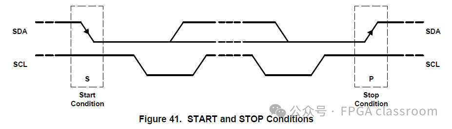
When SDA goes low and SCL is high, it indicates the START condition.
When SDA goes high, SCL is high, it indicates the STOP condition.
Because it specifies the START and STOP conditions, it requires that when SDA transmits data, the SCL must be low at the data edge, otherwise it will be misinterpreted as a START or STOP condition.
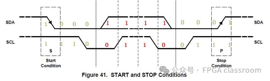
To ensure the above waveform requirements, I divided the model into 4 stages, as shown in the figure below.
Then, according to the manual, to change the output voltage of the DAC5571, we need to send the following data frame:
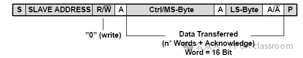
Where S is the START condition,
SLAVE ADDRESS = {6’b100110,A0}, the value of A0 is determined by the voltage at the chip’s A0 pin.
R/W = 0, because we need to write the data representing the voltage.
A represents the ACK signal, the direction is from the chip to the FPGA. Since we are preparing to write a simple driver, we will not process the ACK signal.
Ctrl/MS-Byte = {4’b0000,d[7:4]}, the high 4 bits are 0000, indicating normal operating state, and the low 4 bits are the high 4 bits of the data d that needs to be converted to voltage.
MS-Byte = {d[3:0],4’b0000}, the high 4 bits are the low 4 bits of datad, and the low 4 bits are invalid, filled with 4’b0000.
The following code is provided, where the core is a shift register. When the start pulse arrives, the waveform is stored for later use. Then, with each rising edge of the clock clk, the waveform is continuously pushed out.
module iic_wr_3bytes( input clk,//4x SCL rate input start,//a pulse start to write output SCL, inout SDA);reg [115:0] dat_tmp;reg [115:0] clk_tmp;reg [115:0] tx_flag;wire [6:0]a;wire [7:0]h;wire [7:0]l;wire r;assign a = 7'b1001100;//{6'b100110,A0}assign r = 1'b0;//0 write,1 readassign h = 8'b0000_1111;//{4'b0000,d[7:4]}assign l = 8'b1111_0000;//{d[3:0],4'b0000}initial begin dat_tmp <= 116'hFFFFF_FFFFF_FFFFF_FFFFF_FFFFF_FFFF; clk_tmp <= 116'hFFFFF_FFFFF_FFFFF_FFFFF_FFFFF_FFFF; tx_flag <= 116'hFFFFF_FFFFF_FFFFF_FFFFF_FFFFF_FFFF;endalways @(posedge clk)begin if (start)begin clk_tmp <= {4'b1110,//iic start 4'b0110,4'b0110,4'b0110,4'b0110,4'b0110,4'b0110,4'b0110,4'b0110,4'b0110, 4'b0110,4'b0110,4'b0110,4'b0110,4'b0110,4'b0110,4'b0110,4'b0110,4'b0110, 4'b0110,4'b0110,4'b0110,4'b0110,4'b0110,4'b0110,4'b0110,4'b0110,4'b0110, 4'b0111};//iic stop dat_tmp <= {4'b1000, {4{a[6]}},{4{a[5]}},{4{a[4]}},{4{a[3]}},{4{a[2]}},{4{a[1]}},{4{a[0]}},{4{ r }},4'bzzzz, {4{h[7]}},{4{h[6]}},{4{h[5]}},{4{h[4]}},{4{h[3]}},{4{h[2]}},{4{h[1]}},{4{h[0]}},4'bzzzz, {4{l[7]}},{4{l[6]}},{4{l[5]}},{4{l[4]}},{4{l[3]}},{4{l[2]}},{4{l[1]}},{4{l[0]}},4'bzzzz, 4'b0001}; tx_flag <= {4'b1111, 4'b1111,4'b1111,4'b1111,4'b1111,4'b1111,4'b1111,4'b1111,4'b1111,4'b0000, 4'b1111,4'b1111,4'b1111,4'b1111,4'b1111,4'b1111,4'b1111,4'b1111,4'b0000, 4'b1111,4'b1111,4'b1111,4'b1111,4'b1111,4'b1111,4'b1111,4'b1111,4'b0000, 4'b1111}; end else begin clk_tmp <= {clk_tmp[114:0],1'b1}; dat_tmp <= {dat_tmp[114:0],1'b1}; tx_flag <= {tx_flag[114:0],1'b1}; endend assign SDA = (tx_flag[115]) ? dat_tmp[115] : 1'bz;assign SCL = clk_tmp[115];endmodule The above writing method is very simple and easy to read, but the downside is that it consumes a lot of reg resources. It is recommended to use the above method when resources are not tight. Carefully examine the above waveform and refine the content. The rewritten driver is as follows.
module iic_wr_3bytes_v2( input clk,//4x SCL rate input start,//a pulse start to write output SCL, inout SDA);wire [6:0]a;wire [7:0]h;wire [7:0]l;wire r;assign a = 7'b1001100;//{6'b100110,A0}assign r = 1'b0;//0 write,1 readassign h = 8'b0000_1111;//{4'b0000,d[7:4]}assign l = 8'b1111_0000;//{d[3:0],4'b0000}reg dat_tmp;reg clk_tmp;reg tx_flag;reg [6:0]cnt;reg [26:0]d;initial begin cnt <= 7'd116; tx_flag <= 1'b1; dat_tmp <= 1'b1; clk_tmp <= 1'b1; d <= 27'b111_1111_1111_1111_1111_1111_1111;endalways @(posedge clk)begin if(start)begin cnt <= 1'b0; end else begin if(cnt != 116)begin cnt <= cnt + 1'b1; end endendwire [1:0]phase;wire [4:0]bit;assign phase = cnt[1:0];assign bit = cnt[6:2];always @(posedge clk)begin if(start)begin d <= {a,r,1'bz,h,1'bz,l,1'bz};//'z' will not really happen,use 'z' for easier understanding. end else if(cnt == 116)begin clk_tmp <= 1'b1; dat_tmp <= 1'b1; tx_flag <= 1'b1; end else begin if(bit==5'd0)begin case(phase) 2'd0:clk_tmp <= 1'b1; 2'd1:clk_tmp <= 1'b1; 2'd2:clk_tmp <= 1'b1; 2'd3:clk_tmp <= 1'b0; endcase end else if(bit==5'd28)begin case(phase) 2'd0:clk_tmp <= 1'b0; 2'd1:clk_tmp <= 1'b1; 2'd2:clk_tmp <= 1'b1; 2'd3:clk_tmp <= 1'b1; endcase end else begin case(phase) 2'd0:clk_tmp <= 1'b0; 2'd1:clk_tmp <= 1'b1; 2'd2:clk_tmp <= 1'b1; 2'd3:clk_tmp <= 1'b0; endcase end if(bit==5'd0)begin case(phase) 2'd0:dat_tmp <= 1'b1; 2'd1:dat_tmp <= 1'b0; 2'd2:dat_tmp <= 1'b0; 2'd3:dat_tmp <= 1'b0; endcase end else if(bit==5'd28)begin case(phase) 2'd0:dat_tmp <= 1'b0; 2'd1:dat_tmp <= 1'b0; 2'd2:dat_tmp <= 1'b0; 2'd3:dat_tmp <= 1'b1; endcase end else begin dat_tmp <= d[26]; if(phase==2'd3)d<={d[25:0],1'b1}; end if(bit==5'd9||bit==5'd18||bit==5'd27)begin tx_flag <= 1'b0; end else begin tx_flag <= 1'b1; end endend assign SDA = tx_flag ? dat_tmp : 1'bz;assign SCL = clk_tmp;endmoduleSimulate both modules and compare the output waveforms:
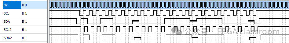
SCL and SDA are the output waveforms of the previous version, SCL2 and SDA2 are the output waveforms of the latter version.
Compare the resource consumption of the two modules:
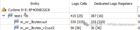
The latter version significantly reduces resource consumption.
I am a teacher of FPGA. Readers can leave a message in the comments about what they want to see. I will handle it when I have time.