1
Component Placement
When placing components, it is essential to follow the signal paths of the schematic and provide space for routing. Additionally, adhere to the following placement rules:
-
Power components should be placed compactly together, with appropriate decoupling to ensure power integrity.
-
Decoupling capacitors should be placed as close as possible to each component.
-
Connectors should be placed at the edges of the board.
-
Follow the schematic flow for high-frequency components.
-
Large storage devices and processors (such as clock generators and controllers) should be placed at the center of the circuit board.
2
Separation of Analog and Digital Modules
To minimize common return paths for analog and digital signals, it is crucial to separate analog and digital modules to prevent mixing of signals.
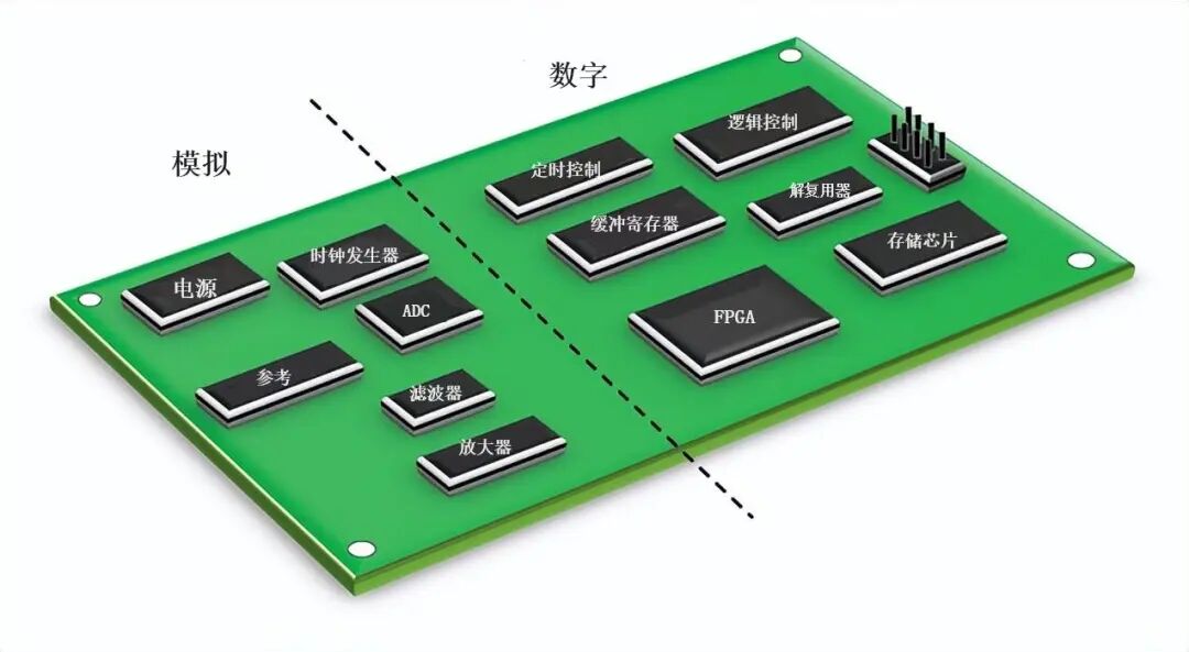
Separation of Analog and Digital Circuits
The above image illustrates an example of separating analog and digital circuits. When dividing the analog and digital sections, keep the following points in mind:
-
It is recommended to install precision analog components, such as amplifiers and reference voltage sources, on the analog plane. The opposite side/digital plane must be used for noisy digital components, such as logic controls and timing blocks.
-
Analog-to-digital converters (ADC) or digital-to-analog converters (DAC) in the system are mixed-signal and have low digital currents, and should be treated similarly to analog components in the analog system.
-
For designs with a large number of high-current ADCs and DACs, it is advisable to separate the analog and digital power supplies. In other words, DVDD should connect to the digital section, while AVCC must connect to the analog section.
-
Microprocessors and microcontrollers can generate significant space and heat. To improve heat dissipation, these components must be placed at the center of the circuit board and close to the circuit blocks they connect to.
3
Trace Routing
Once all components are correctly placed in optimal positions and an appropriate ground plane is established, most traces will naturally follow the correct paths. However, keep the following guidelines in mind when routing traces:
-
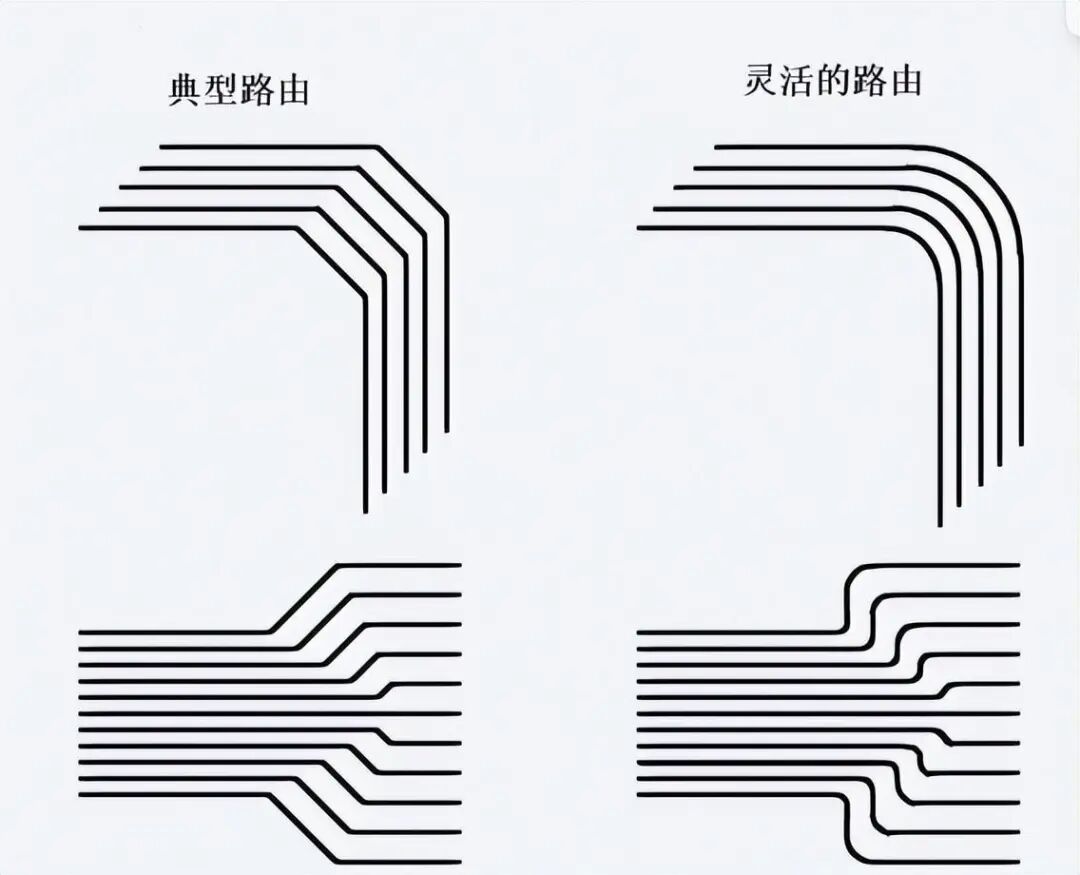
Signal paths should be as direct and short as possible.
-
Layers with high-speed signal paths should have a ground layer adjacent to ensure proper return signals.
-
High-speed circuits are particularly sensitive and require adherence to the signal paths laid out in the schematic.
-
Reduce inductance in power routing by using short, direct, and wide traces.
-
Avoid creating antennas when routing traces and vias.
-
Power routing should be short, compact, and utilize wide traces.
-
Routing needs to maintain isolation between digital and analog circuit elements.
-
Grounding is crucial, especially for traces connecting digital and analog partition areas.
4
Power Modules
Power is a critical component of the circuit and needs to be handled carefully. Generally, power modules must be placed close to the components they supply while being isolated from the rest of the circuit.
When devices in complex systems have many power pins, dedicated power modules can be used for analog and digital sections to prevent noisy digital interference.
To reduce inductance and prevent current limitations, power lines should be short and straight, using wide traces.
5
Decoupling
One of the key factors engineers must consider to meet the performance required by the system is the Power Supply Rejection Ratio (PSRR). The performance of the device is ultimately determined by PSRR, which assesses the sensitivity of the device to power variations.
To maintain an ideal PSRR, it is necessary to prevent high-frequency energy from entering the device. To achieve this, a combination of electrolytic and ceramic capacitors can effectively isolate the device’s power from the high-impedance ground layer.
Effective decoupling is essential for maintaining a low-noise environment during circuit operation. The basic rule is to provide the shortest possible path to facilitate current return.
Here are some common decoupling methods:
-
Low-inductance ceramic capacitors are used to reduce high-frequency noise, while electrolytic capacitors act as charge reservoirs to reduce low-frequency noise on the power supply. Additionally, ferrite beads are optional but can enhance high-frequency noise isolation and decoupling.
-
Decoupling capacitors should be placed as close as possible to the power pins of the device. To reduce additional series inductance, these capacitors should be connected to the majority of the low-impedance ground layer using vias or short traces.
-
The power pins of the device should be as close as possible to the device. Smaller capacitors (typically 0.01F to 0.1F) should be used to avoid unstable operation when multiple outputs switch simultaneously. The distance between the electrolytic capacitor and the device’s power pins should not exceed one inch (averaging 10F to 100F).
-
Decoupling capacitors can be connected to the ground layer using vias close to the device’s GND pins to simplify the structure instead of building traces.
Specific examples can be seen in the following image:
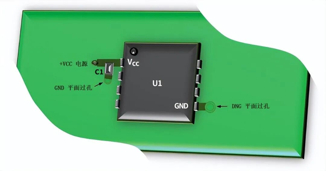
Decoupling Techniques for Power Pins
6
PCB Layering
Before routing the PCB, it is essential to consider the layering of the PCB, as it can affect the return paths allowed by the system design.
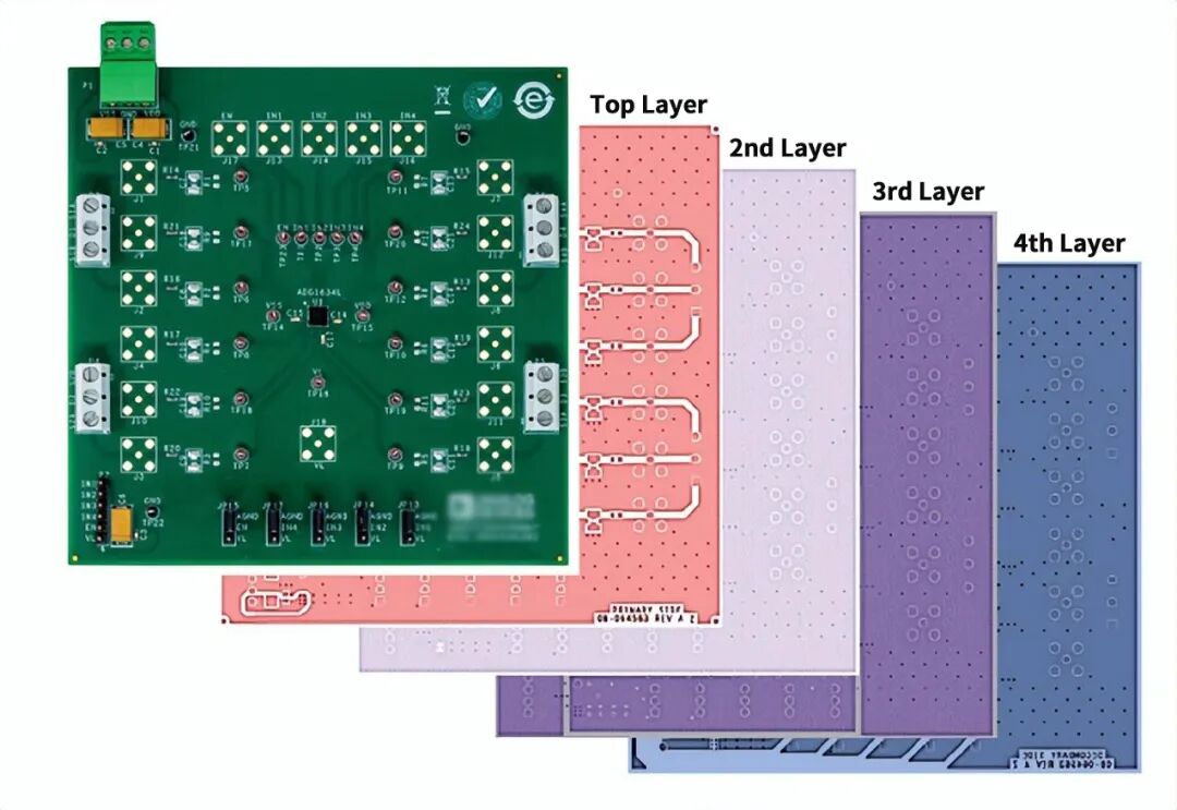
4-Layer PCB Example
The above image provides a visual representation of the various layers of the circuit board. The following image details the typical setup of a PCB:
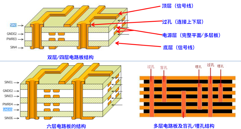
Typical PCB Layers
High-performance data acquisition systems should typically include four or more layers. Auxiliary signals are usually placed on the bottom layer, while digital/analog signals are typically on the top layer. The second layer (also known as the ground layer) serves as a reference layer for impedance-controlled signals, reducing IR drop and protecting the digital signals on the top layer. The power layer is located on the third layer.
Due to the additional inter-layer capacitance they provide, the power and ground layers must be close to each other to decouple the power at high frequencies.
7
PCB Copper Resistance
The resistance of copper is also important in mixed-signal PCB layouts, as copper traces can form good interconnections and ground layers.
Most PCBs use 1 oz copper, but high-power sections may use 2 or 3 oz copper. The resistivity of copper at 25°C is 1.724X10 -6 Ω/cm.
A common thickness for 1 oz copper foil is 0.036 mm (0.0014 in), with a resistance of 0.48 mΩ/sq. For example, the resistance/length of a commonly used 0.25 mm (10 mil) wide trace on a PCB is approximately 19 mΩ/cm (48 mΩ/in).
The resistance of PCB traces can be a source of error for mixed-signal ICs. For a 16-bit ADC with a 5 kΩ input resistance, driven through 5 cm of 0.25 mm wide 1 oz copper, the trace resistance is 0.1 Ω, forming a voltage divider with the 5 kΩ load, resulting in a 0.1 error/5 k (approximately 0.0019%), which exceeds the 1 LSB (0.0015%) of the 16-bit ADC, as shown below:
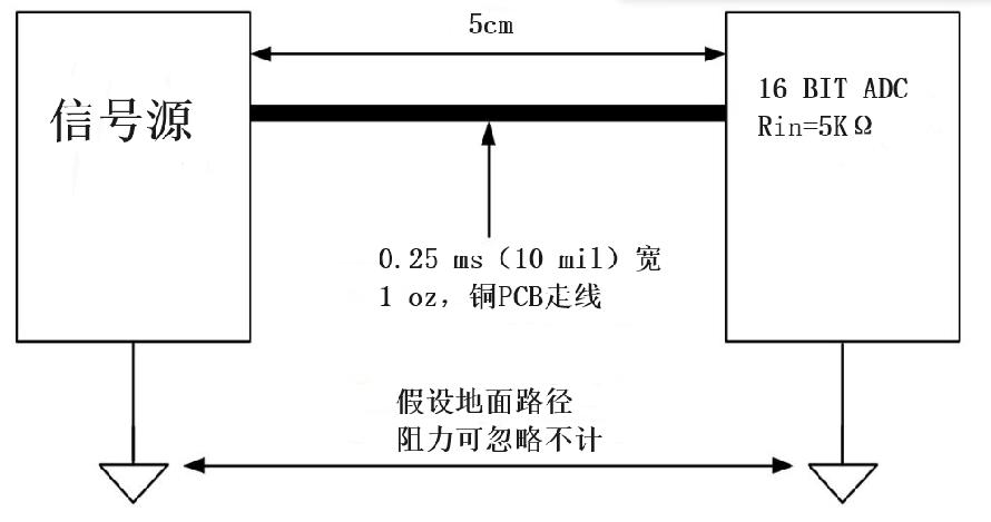
PCB trace resistance is a significant factor in mixed-signal PCBs.
In practical applications, this may be more severe as it neglects return paths and the 0.4%/°C temperature coefficient of copper at 25°C. When dealing with low-impedance precision circuits, the resistance of copper is crucial for successful design.
8
Grounding
01
Single Ground Layer
The best approach for a mixed-signal system with a single low digital current ADC or DAC is to use a single solid ground layer.
To understand the importance of a single ground layer, it is necessary to analyze return currents. The term “return current” describes the current that completes the circuit loop and flows back to ground. Each return path must be followed throughout the PCB layout to avoid mixed-signal interference.
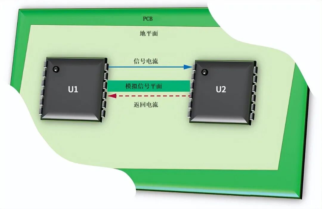
Return currents in systems using solid ground layers
The simple circuit in the above image illustrates the advantages of a single solid ground layer compared to multiple ground layers. There exists a return current equal to the signal current but in the opposite direction. When the return current flows back to the source in the ground layer, it will take the path of least resistance.
The path of least resistance (usually a straight line between the device ground references) will follow the return current for low-frequency transmissions. However, a portion of the return current will attempt to return along the signal path for higher frequency transmissions. This is due to the lower impedance and smaller loop created between the output and return currents along that path.
02
Separate Analog and Digital Grounds
Another typical strategy is to divide the ground layer into two halves: an analog ground layer and a digital ground layer. This is suitable for more complex systems with a large number of mixed-signal components and high digital current requirements. The following image illustrates a system with divided ground layers.
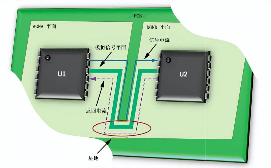
Return currents in systems with separated ground layers
Eliminating ground layer breaks and allowing return currents to take a more direct path back through a star ground connection is the simplest way to achieve overall grounding for systems with separate ground layers. In mixed-signal layouts, the intersection of the analog and digital ground layers is referred to as star grounding.
Star grounding can connect typical thin continuous connections between the analog and digital ground layers in common systems. For more complex systems, star grounding is often performed by diverting jumpers to ground connections.
Since star grounding does not carry current, high-current connectors and jumper diverters are not required. The primary function of star grounding is to ensure that the reference levels of the two grounds are the same.
On the other hand, since star grounding connects two grounds at one point, mixed-signal devices with AGND and DGND pins can connect to their respective ground layers. This separates precision analog circuits from high-noise digital currents that flow through the digital power supply back to the digital ground.
Multilayer PCBs must achieve complete isolation of AGND and DGND planes.
9
Electromagnetic Interference Shielding
After addressing ground bounce, crosstalk, power noise, and other interferences, circuits may still suffer from electromagnetic interference (EMI). This can lead to various issues such as:
-
Interference with wireless communications
-
Communication interruptions
-
Corruption of sensor data
-
Component failures
-
Software errors and malfunctions
One effective way to address EMI is to use sufficient metal shielding. Ideally, the shielding should form a Faraday cage, covering the circuit from all six sides and the ground layer.
While using shielding can block most incoming EMI, thermal cooling issues must also be addressed, and signal inputs and outputs must be allowed.


Screenshots from the 400G Collection E-book