Unfortunately, my calibration source has malfunctioned. In the spirit of diligence and learning, I have thoroughly studied the principles of the FLUKE 5700 DAC and plan to document my learning process while also creating a test board for practical application. The FLUKE 5700 indeed uses PWM (Pulse Width Modulation) for DAC output: (1) It only has a positive output; the negative output is obtained by switching the output signal inversion through an internal relay. (2) It is actually a combination of two DACs.
For example, if the duty cycle of the first channel is 10%, and the second channel is 50%, the overall average voltage is:
(0.1 x 13V) + (0.5 x 0.78 mV) = 1.300390V
The duty cycle resolution is 0.0024%, which makes the resolution of the first channel 0.309 mV, and the second channel’s resolution is 18.5 nV.
Due to the stability of the PWM output, there are no lost pulses, and thus the least significant bit is not lost, so feedback correction for the second channel is not necessary.
(3) The ranges of 11V and 22V are generated by the DAC component,
2.2V range is generated on the switching matrix component by dividing the 11V range of the DAC component by a factor of five using resistors. The switching matrix and the relays on the analog motherboard route the 2.2V range output to the calibration terminal.
The 220 mV range is an extension of the 2.2V range. The switching matrix component generates the 220 mV range by dividing the 2.2V range by a factor of ten using resistors. The switching matrix and the relays on the analog motherboard route the 220 mV range output to the front panel terminal. The 220V range is generated by the DAC and power amplifier components. The power amplifier amplifies the 11V range of the DAC component by a factor of 20 to generate the 220V range. The output of the power amplifier is sent to the high-voltage control component (A14), where a relay connects it to PA OUT DC. The PA OUT DC line is routed through the switching matrix and relays on the analog motherboard to the terminal.
The 1100V range is generated by the high-voltage/large current component (A15) working in conjunction with the power amplifier and high-voltage control components. The signal from the 11V range of the DAC component is introduced to the high-voltage/large current component, which amplifies it with a gain of -100 to produce the 1100V range. Essentially, the high-voltage output is obtained from the high-voltage AC signal generated by the high-voltage control component working with the power amplifier component through rectification and filtering. Today, I tested using the most basic gate circuit chip counter and flip-flop through the policy software, with a design resolution of 12 bits and a base clock of 10 MHz, using switches to simulate IO levels.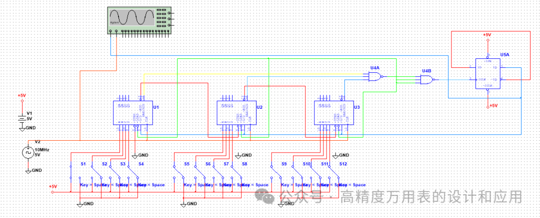 10M/2^12=2441.4, this is the DAC’s update rate, outputting once every 4096 pulses, which is approximately every 409.6uS, with a DAC value of 0x001, the output waveform is
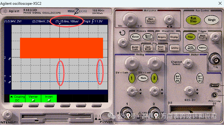 amplifying the pulse width
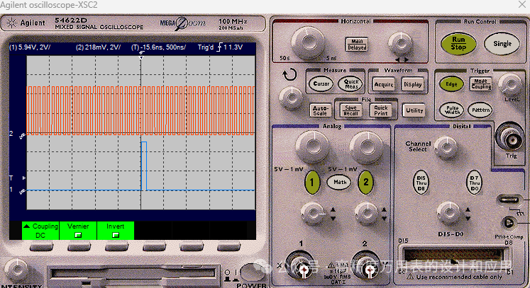 output waveform for 0xFFF
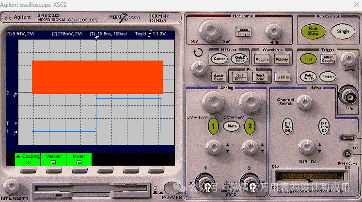 amplifying the pulse
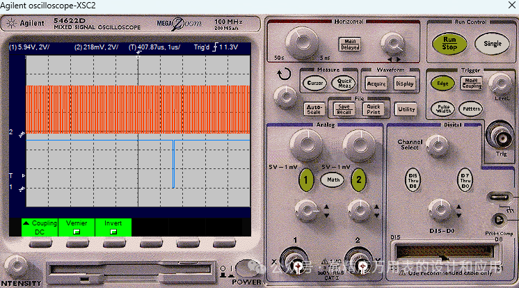 The DAC uses a PWM output method with a low rate but high accuracy, making it suitable for calibration sources. However, the power supply for the pulse signal must be very stable; otherwise, deviations will occur. The next step is to simulate the rectification and filtering circuit, and I will still use the two-channel superposition method to attempt a 24-bit resolution DAC test.