MCUMicro Classroom
CKS32K148 PDB
Issue 58 2025.08.05
The Programmable Delay Block (PDB) provides a controllable delay from the trigger source to the ADC hardware trigger input, with the trigger source coming from internal, external triggers, or a programmable interval clock. The PDB can optionally provide pulse outputs, which can be used as sampling windows in the Comparator (CMP).
The CKS32K148 has two PDBs, each with 4 channels, one pulse output, and one trigger. Each channel has 8 pre-triggers. Therefore, one PDB module can trigger up to 32 ADC input channels at once.

Structure and Block Diagram
The block diagram of the PDB in the CKS32K148 series MCU is shown below, which can be roughly divided into six parts.
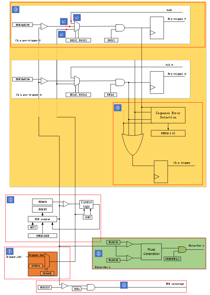
Figure 1 AIPS Result Block Diagram
① Trigger Source Selection: The trigger source selection of the PDB is determined by the TRGSEL bit in the PDB_SC register, which can be a software trigger – achieved by writing 1 to the SWTRIG bit of the PDB_SC register; or an external trigger source – such as the external trigger pin Trigger_In0.
② Counter Section: The clock source of the PDB is divided by the division factor selected by the PRESCALER bit in the PDB_SC register, and the multiplication factor is selected by the MULT bit in the PDB_SC register. The counter then begins to operate. The current count value of the counter can be read from the counter register PDB_CNT. The period of the counter is specified by the PDB_MOD modulus register, and when the counter reaches this value, it will be reset to zero.
The control logic of the counter is implemented through the CONT bit in the PDB_SC register: when this bit is inactive, the counter is reset to zero when it reaches the period value, until the next trigger occurs to restart counting; when this bit is active, the counter automatically restarts when it reaches the period value.
③ Pre-trigger Output Section: The PDB channel n (n = 0 ~ 3) pre-trigger output 0~m (with a maximum value of 7), each pre-trigger output connects to the ADC hardware trigger selection and hardware trigger input. The pre-trigger can be enabled or disabled using the PDB channel pre-trigger enable (CHn1C1[EN[m]]).
For convenience, we define the trigger input event as: detecting a rising edge on the selected trigger input source, or selecting the software trigger and writing 1 to the software trigger bit (SC[SWTRIG]). The pre-trigger source output corresponds to three situations:
a) When the trigger input event occurs, the pre-trigger m is set after 2 peripheral clock cycles. In this case, CHnC1[TOS[m]] needs to be cleared.
b) Using the channel delay register CHnDLYm to specify the delay value, when the counter count value reaches this value, the pre-trigger m is set after two peripheral clock cycles. In this case, CHnC1[TOS[m]] needs to be set.
c) The PDB is configured for back-to-back operation, which allows the completion of the ADC conversion to trigger the next PDB channel pre-trigger and trigger output. In other words, the pre-trigger m-1 will set the pre-trigger output m after the Ack signal generated by the completion of the ADC conversion. In this case, CHnC1[BB[m]] needs to be set.
④ Trigger Output Section: The pre-trigger output is used to preprocess the ADC block before the actual trigger occurs. When the ADC receives the rising edge of the trigger, it will start conversion based on the prerequisites determined by the pre-trigger. The pre-trigger and trigger output of PDB channel n are shown in the figure below.
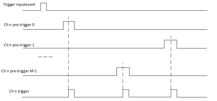
Figure 2 Pre-trigger Output and Trigger Output
If the pre-trigger of PDB channel n is set while setting a new pre-trigger m, a PDB channel sequence error flag (CHnS[ERR[m]] is set). If the PDB sequence error interrupt is enabled, a sequence error interrupt will occur. Sequence errors are usually caused by the delay m being set too short, and pre-trigger m being set before the previous triggered ADC conversion is completed. For example, if pre-trigger m-1 is set and the ADC conversion process has not yet finished, setting pre-trigger m will cause a sequence error.
⑤ Pulse Output Section: The PDB can generate pulse outputs with configurable widths. When the PDB counter reaches the value set in PonDLY[DLY1], the pulse output goes high; when the PDB counter reaches the value set in PonDLY[DLY2], the pulse output goes low. PonDLY[DLY2] can be set to be greater than or less than the value in PonDLY[DLY1].
⑥ Interrupt Section: The interrupt delay register PDB_IDLY specifies the delay value for the PDB interrupt, which can be used to schedule an independent interrupt at a certain point in the PDB cycle. If the interrupt is enabled (PDB_SC[PDBIE] is set), a PDB interrupt will occur when the counter equals IDLY.
PDB Delay Trigger ADC Multi-channel Experiment
The most commonly used function of the CKS32K148 PDB is to provide a hardware trigger source for the ADC. Here we demonstrate the PDB delay trigger ADC function, specifically the situation b) mentioned earlier – using the channel delay register CHnDLYm to specify the delay value, when the counter count value reaches this value, the pre-trigger m is set after two peripheral clock cycles.
As mentioned earlier, each PDB module has 4 channels, 1 trigger, and one pulse output, with each channel having 8 pre-trigger outputs. Here we only use 1 channel, 1 trigger, and 8 pre-trigger outputs to trigger the 8 input channels of the ADC. To avoid PDB sequence errors, it is necessary to ensure sufficient delay between pre-triggers.
The programming key points are as follows:
1. Enable the relevant peripheral clocks, such as ADC, PDB, etc., and configure the pins used.
status = CLOCK_DRV_Init(&clockMan1_InitConfig0);
DEV_ASSERT(status == STATUS_SUCCESS);
status = PINS_DRV_Init(NUM_OF_CONFIGURED_PINS0, g_pin_mux_InitConfigArr0);
DEV_ASSERT(status == STATUS_SUCCESS);
2. Configure the ADC structure parameters and input channels. Here we only show the configuration functions for the first 2 channels.
ADC_DRV_ConfigConverter(INST_ADC_0, &ADC_0_ConvConfig0);
PDB_DRV_ConfigAdcPreTrigger(INST_PDB_0, 0U, &pdb_1_adcTrigConfig0);
PDB_DRV_ConfigAdcPreTrigger(INST_PDB_0, 0U, &pdb_1_adcTrigConfig1);
/*** ADC Initialization Structure ***/
const adc_converter_config_t ADC_0_ConvConfig0 = {
.clockDivide = ADC_CLK_DIVIDE_4,
.sampleTime = 255U,
.resolution = ADC_RESOLUTION_12BIT,
.inputClock = ADC_CLK_ALT_1,
.trigger = ADC_TRIGGER_HARDWARE,
.pretriggerSel = ADC_PRETRIGGER_SEL_PDB,
.triggerSel = ADC_TRIGGER_SEL_PDB,
.dmaEnable = false,
.voltageRef = ADC_VOLTAGEREF_VREF,
.continuousConvEnable = false,
.supplyMonitoringEnable = false
};
The key is to configure the ADC for hardware triggering, with both the pre-trigger source and trigger source being PDB, and to disable continuous mode. Configure the 8 ADC input channels: specify external/internal input channels, and enable conversion complete interrupts for each channel.
3. PDB Counter Configuration and Enable
PDB_DRV_Init(INST_PDB_0, &pdb_1_timerConfig0);
PDB_DRV_Enable(INST_PDB_0);
/*** PDB Counter Initialization Structure ***/
const pdb_timer_config_t pdb_1_timerConfig0 = {
.loadValueMode = PDB_LOAD_VAL_IMMEDIATELY,
.seqErrIntEnable = false,
.clkPreDiv = PDB_CLK_PREDIV_BY_128,
.clkPreMultFactor = PDB_CLK_PREMULT_FACT_AS_10,
.triggerInput = PDB_SOFTWARE_TRIGGER,
.continuousModeEnable = true,
.dmaEnable = false,
.intEnable = false,
.instanceBackToBackEnable = false,
};
The parameter loadValueMode is used to select the loading mode, controlling the registers that operate the PDB (such as modulus registers, interrupt delay registers, etc.) to become valid simultaneously. The values written to these registers will first be updated to their buffers, so the loading mode is used to select the condition under which the buffer values are updated to the internal registers. Here we choose the default value, which is to immediately update the buffer loading value.
The parameter seqErrIntEnable is used to set whether to enable the PDB sequence error interrupt. Here we disable it.
The parameter clkPreDiv is used to select the pre-division factor. Here we set it to 128.
The parameter clkPreMultFactor is used to select the multiplication factor. Here we set it to 10.
The parameter triggerInput is used to select the trigger input source. Here we choose software triggering.
The parameter continuousModeEnable is used to select whether to enable continuous mode. We enable continuous mode, so when the counter reaches the period value, it automatically restarts counting from zero.
The parameter dmaEnable is used to select whether to enable DMA. If DMA is enabled, when the PDB counter reaches the delay value specified by the interrupt delay register PDB_IDLY, the PDB interrupt flag is set, and the PDB requests a DMA transfer. Here we disable DMA.
The parameter intEnable is used to select whether to enable the counter interrupt. A counter delay interrupt will only occur when DMA is disabled. Here we disable the counter interrupt.
The parameter instanceBackToBackEnable is used to select whether to enable back-to-back operation, corresponding to the pre-trigger output situation c) mentioned earlier. Here we disable back-to-back operation.
4. Configure the PDB Counter Period Value
calculateIntValue(&pdb_1_timerConfig0, PDLY_TIMEOUT, &delayValue0);
PDB_DRV_SetTimerModulusValue(INST_PDB_0, (uint32_t) delayValue0);
PDLY_TIMEOUT is the user-defined period value, set to 1s. The calculateIntValue function converts the user-defined counter period into the corresponding hexadecimal number based on the counter’s clock frequency, and then writes this hexadecimal number into the PDB_MOD register.
5. Configure the PDB Pre-trigger Outputs (only showing the configuration functions for the first two pre-trigger outputs of channel 0)
PDB_DRV_ConfigAdcPreTrigger(INST_PDB_0, 0U, &pdb_1_adcTrigConfig0);
PDB_DRV_ConfigAdcPreTrigger(INST_PDB_0, 0U, &pdb_1_adcTrigConfig1);
/*** Pre-trigger Output Configuration Structure ***/
const pdb_adc_pretrigger_config_t pdb_1_adcTrigConfig0 = {
.adcPreTriggerIdx = 0U,
.preTriggerEnable = true,
.preTriggerOutputEnable = true,
.preTriggerBackToBackEnable = false
};
The above parameters are: pre-trigger output index (0~7), whether to enable pre-trigger, whether to enable pre-trigger output, and whether to enable back-to-back operation. The other pre-trigger outputs have the same configuration except for the output index.
6. Set the Pre-trigger Delay Values
PDB_DRV_SetAdcPreTriggerDelayValue(INST_PDB_0, 0UL, 0UL,(uint32_t) delayValue0 / 9);
PDB_DRV_SetAdcPreTriggerDelayValue(INST_PDB_0, 0UL, 1UL,(uint32_t) delayValue0 / 8);
PDB_DRV_SetAdcPreTriggerDelayValue(INST_PDB_0, 0UL, 2UL,(uint32_t) delayValue0 / 7);
PDB_DRV_SetAdcPreTriggerDelayValue(INST_PDB_0, 0UL, 3UL,(uint32_t) delayValue0 / 6);
PDB_DRV_SetAdcPreTriggerDelayValue(INST_PDB_0, 0UL, 4UL,(uint32_t) delayValue0 / 5);
PDB_DRV_SetAdcPreTriggerDelayValue(INST_PDB_0, 0UL, 5UL,(uint32_t) delayValue0 / 4);
PDB_DRV_SetAdcPreTriggerDelayValue(INST_PDB_0, 0UL, 6UL,(uint32_t) delayValue0 / 3);
PDB_DRV_SetAdcPreTriggerDelayValue(INST_PDB_0, 0UL, 7UL,(uint32_t) delayValue0 / 2);
Previously, we set the PDB period to 1s, so the delay between pre-trigger output 1 and pre-trigger output 0 is 1 * (1/8 – 1/9) = 13.88ms. Similarly, the delay between pre-trigger 2 and pre-trigger 1 is 17.925ms, between pre-trigger 3 and pre-trigger 2 is 11.9ms, between pre-trigger 4 and pre-trigger 3 is 16.65ms, between pre-trigger 5 and pre-trigger 4 is 25ms, between pre-trigger 6 and pre-trigger 5 is 41.65ms, and between pre-trigger 7 and pre-trigger 6 is 83.3ms.
7. Execute Load Command, Enable Software Trigger
PDB_DRV_LoadValuesCmd(INST_PDB_0);
PDB_DRV_SoftTriggerCmd(INST_PDB_0);
After executing the load command, the previously set register values (PDB_MOD, PDB_CHnDLYm) are immediately updated from the buffer to the internal registers. After the software trigger of the PDB, the counter starts working.
8. Enable ADC Interrupt
INT_SYS_InstallHandler(ADC0_IRQn, &ADC0_IRQHandler, (isr_t*) 0);
INT_SYS_EnableIRQ(ADC0_IRQn);
9. Write Interrupt Service Function: Get ADC Results in the Interrupt and Toggle IO Level
void ADC0_IRQHandler(void)
{
ADC_DRV_GetChanResult(INST_ADC_0, 0UL, (uint16_t *)&adcRawValue0[0]);
ADC_DRV_GetChanResult(INST_ADC_0, 1UL, (uint16_t *)&adcRawValue0[1]);
ADC_DRV_GetChanResult(INST_ADC_0, 2UL, (uint16_t *)&adcRawValue0[2]);
ADC_DRV_GetChanResult(INST_ADC_0, 3UL, (uint16_t *)&adcRawValue0[3]);
ADC_DRV_GetChanResult(INST_ADC_0, 4UL, (uint16_t *)&adcRawValue0[4]);
ADC_DRV_GetChanResult(INST_ADC_0, 5UL, (uint16_t *)&adcRawValue0[5]);
ADC_DRV_GetChanResult(INST_ADC_0, 6UL, (uint16_t *)&adcRawValue0[6]);
ADC_DRV_GetChanResult(INST_ADC_0, 7UL, (uint16_t *)&adcRawValue0[7]);
PINS_DRV_TogglePins(LED_PORT, 1 << LED0);
adc0ConvDone = true;
}
Thus, the routine for the PDB multi-channel delay triggering ADC is basically completed. After compiling the program and burning it to the development board, the PDB pre-trigger will set and trigger the ADC conversion completion, entering the interrupt to toggle the IO level. Users can verify whether the delay value is consistent with expectations based on the captured IO level waveform. Additionally, if users want to see the ADC conversion values, they can enable the serial port and print the results in the main function’s while loop based on the adc0ConvDone flag, which will not be elaborated here.
// Transferred from Zhongke Core MCU
Contact Us:
Address: Building B, Xinxin Tiandi Industrial Park, Xiawei Garden, Gushu 2nd Road, Xixiang Street, Bao’an District, Shenzhen
Phone: 15989378236
Email: [email protected]