The following question was asked by a VIP student from the Cortex-A72 training camp: After completing the single-core CPU PR, how do I output the data to TOP for multi-core hierarchy integration?
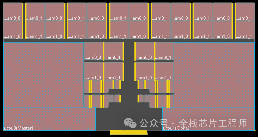
Answer: After completing the single-core CPU, you need to output library files such as SDC, DEF, LEF, GDS, Netlist, LIB, etc., and then design the hierarchy for TOP.
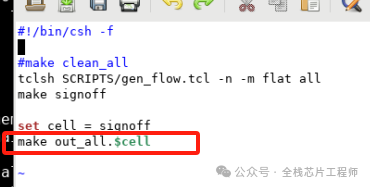
For example, the command to extract lib is as follows:
do_extract_model -view $VIEW ./$DESIGN.$VIEW.libFor other commands, please refer to the server scripts!
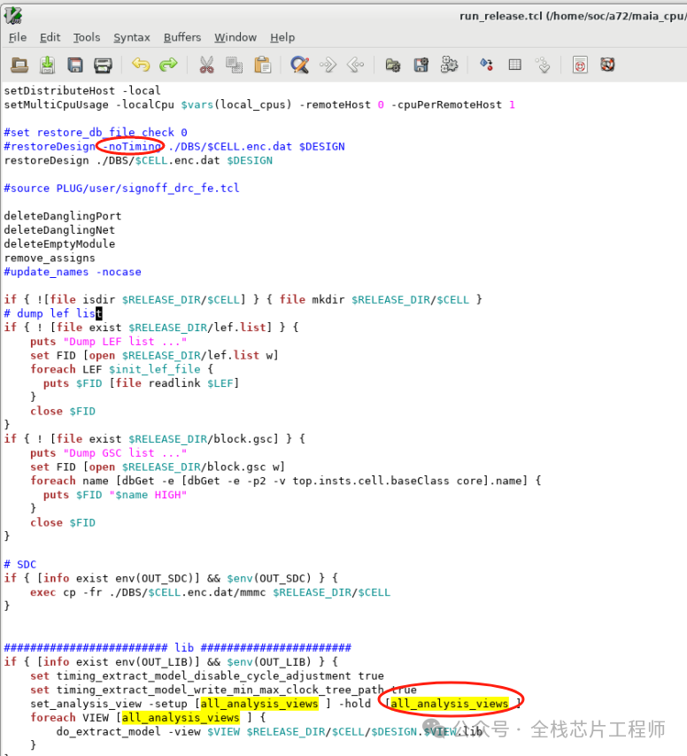
A student from the Cortex-A72 training camp asked: I want to output lib from invs, but during the release, the view was completely removed. I am not sure what happened?
Answer: The reason for the empty analysis_view is due to -noTiming, as shown in the figure below:
A student from the Cortex-A72 training camp asked: At which step is the pin assigned during partitioning?
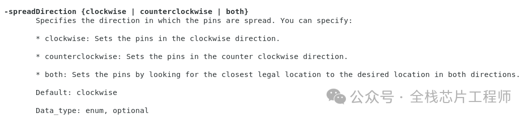
Answer: Just add the following script during partitioning to editPin:
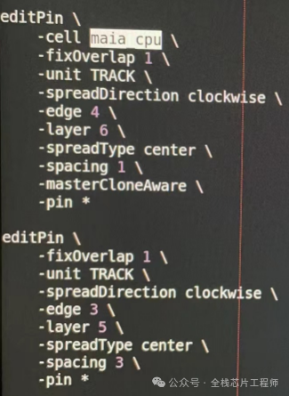
For example:
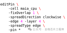
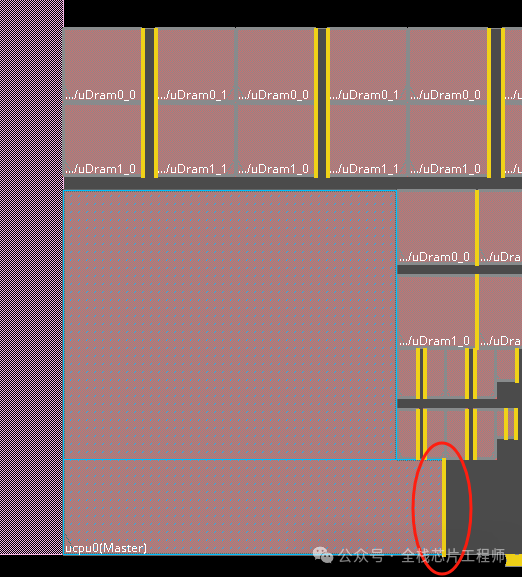
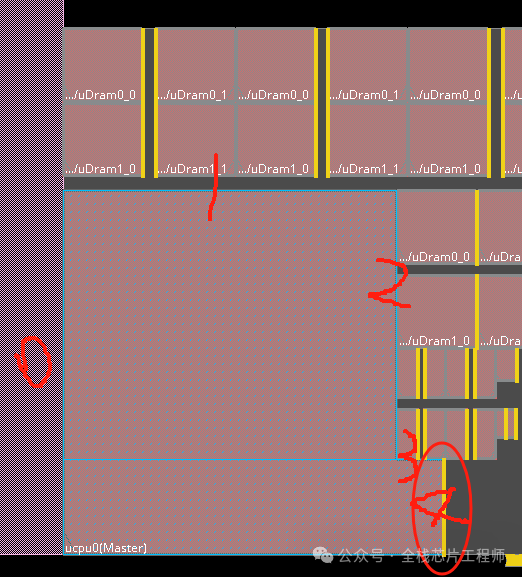
The clockwise is the order of the pins.
A student from the Cortex-A72 training camp asked: Did I write the coordinates wrong below?
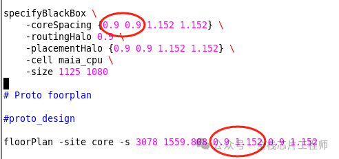
Answer: The format during floorplan is as shown in the figure below, left bottom right top, but the order for specifyBlackBox’s -coreSpacing is left right up down!
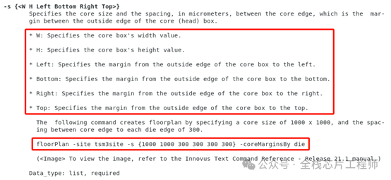
A student from the Cortex-A72 training camp asked: What considerations were taken to determine the values 0.9 and 1.152?
Answer: 1.152 is the height of the two sites, and 0.9 should also be a multiple of the width of the left and right sites or the met pitch multiple.
“ 12nm Process, 2.5GHz Frequency, Cortex-A72 Backend Practical Training”
01
Cortex-A72 Processor—Digital Backend Practice
This project is a practical training project, focusing on low-power UPF design, with backend parameters as follows:
Process:12nm
Frequency:2.5GHz
Resources:2000_0000 instances
Flow:Partition Flow
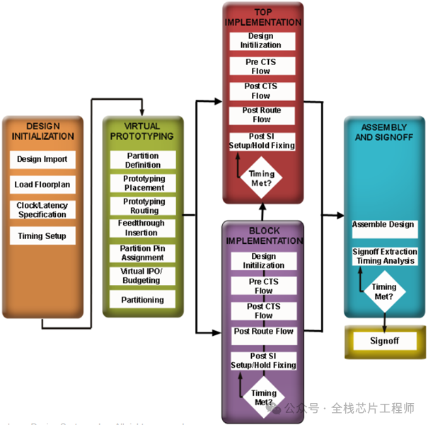
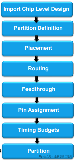
Partition Steps:
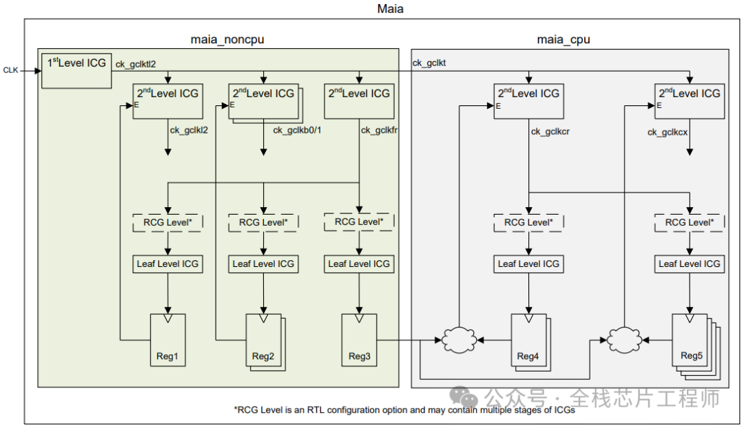
Clock Structure Analysis:
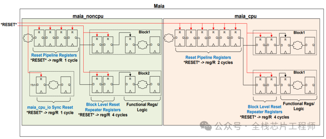
Placement Structure Analysis:
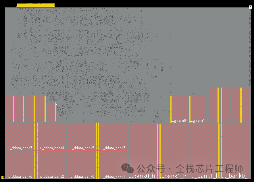
Cortex-A7 Single Core:
Gates=240291 Cells=118421
Cortex-A72 Single Core:
Gates=3125649 Cells=1207766
28nm Cortex-A7 Single Core:
12nm Cortex-A72 Single Core:
Area=486100.9 um^2
Cortex-A72 Processor Partition Flow:
Cortex-A7 Processor:
DDR3/4 Practical Course
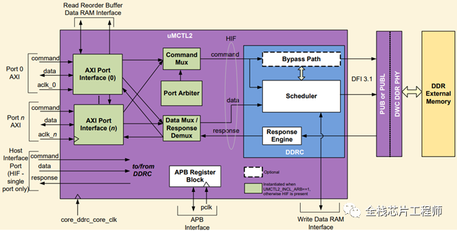
The course instructor is a 10-year IC design expert with in-depth research and unique insights into DDR chip design. Through vivid cases and in-depth analysis, he helps students master the core skills and practical experience of DDR design.
This training will adopt a practical case teaching method, allowing you to master the techniques and methods of DDR chip design through hands-on operation. We will provide real DDR chip design projects for you to participate in and exchange experiences with other students to improve design levels together.
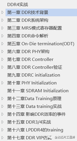
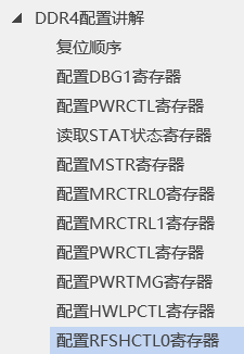
Course Highlights:
-
Design verification using mainstream DDR IP
-
Analyzing protocols in practice, replacing tedious protocol explanations
-
Cases based on already TO chip designs
-
Sharing years of DDR debugging experience
-
Building DDR verification environments
Join the knowledge planet and become part of the chip design knowledge treasure!
Knowledge Planet of SoC Training Camp
SoC Full Process Design Service
Chip training (real project) introduction:
-
Nationally unique low-power image SoC front-end, mid-end, and back-end full-process practical training
-
DDR4/3 project practical training
-
ARM Cortex-A72 processor 12nm PR practical training
-
ARM Cortex-A72 processor 12nm DFT practical training
-
Cross-clock domain RTL design and CDC practice
-
UPF design and low-power simulation practice
Chip Design Service introduction:
-
Providing SoC, MCU, ISP, CIS, etc. chip design, verification, DFT design services
-
Providing DDR/PCIE/MIPI/CAN/USB/ETH/QSPI/UART/I2C IP design
-
Providing back-end design for 7nm, 12nm, 28nm, 40nm, 55nm, 65nm, 90nm
-
Providing customized chip design services and design training for universities and enterprises
【Let every student be able to design an SoC/MCU chip】
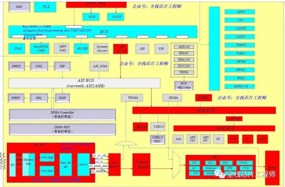
【The only one on the internet】Jingshi SoC is a low-power ISP image processing SoC used for 【chip full-process design training】, using a low-power RISC-V processor, built-in ITCM SRAM, DTCM SRAM, integrating IPs including MIPI, ISP, USB, QSPI, UART, I2C, GPIO, Ethernet MAC controller, designed using SMIC40 process.
-
High-speed interface Verilog design implementation -
From image algorithm to RTL design implementation -
MIPI, ISP Verilog implementation and simulation -
Lint, CDC checks and UVM verification -
Post-simulation
The content of just the front-end course is equivalent to 5-6 courses from other training institutions.
-
DFT design (chip-level) -
Synthesis logic synthesis (chip-level) -
Low-power UPF design, CLP technology -
Formal verification and other technologies
(3) In the SoC backend course, you will learn
-
Low-power design
-
Layout and routing (low-power FF flow) -
StarRC/QRC -
STA/Tempus -
Power analysis -
DRC/LVS design
The content of just the backend course is equivalent to 3-4 courses from other training institutions.
Join the knowledge planet and become part of the chip design knowledge treasure!
Knowledge Planet of SoC Training Camp