
Today, Pi Zi Heng introduces the actual capture of Flash signal waveforms to examine the AHB read access conditions under the FlexSPI peripheral of i.MXRT.
In the previous article “Actual Capture of Flash Signal Waveforms to Examine AHB Read Access Conditions Under the FlexSPI Peripheral of i.MXRT (With Prefetch)” Pi Zi Heng captured the timing waveform of AHB read access corresponding to the Flash end with Cache disabled but Prefetch enabled. We learned that the Prefetch function of FlexSPI indeed improves Flash access efficiency to some extent, but the AHB RX Buffer is limited to a maximum of only 1KB (for i.MXRT1050), and cannot be split into smaller buffers to cache data from different Flash addresses (for the same AHB master). Thus, for repeated accesses to multiple different small data blocks in the Flash space in the code, the Prefetch mechanism does not significantly improve access efficiency.
To address this inefficient situation of frequently accessing non-contiguous Flash address spaces, the ARM Cortex-M7 core provides a solution: the L1 Cache technology. Today, Pi Zi Heng will continue to measure the Flash AHB read access conditions with L1 Cache enabled (this article mainly focuses on D-Cache):
1. Cache Function of Cortex-M7
For the Cortex-M series family (M0+/M3/M4/M7/M23/M33/M35P/M55), L1 Cache exists only on the Cortex-M7 and Cortex-M55 cores. In simple terms, L1 Cache is configured specifically for high-performance cores, and currently, the i.MXRT1xxx series microcontrollers are all based on the Cortex-M7 core.
Below is the core system block diagram of i.MXRT1050. It can be seen that it integrates a 32KB D-Cache, which is connected via the AXI64 bus to the SIM_M7 and SIM_EMS modules, and ultimately connected to the FlexSPI module via the AHB bus. Therefore, the AHB read access to Flash can be accelerated by the D-Cache.
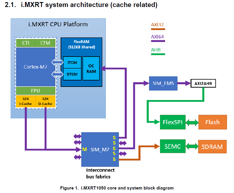
Details about the D-Cache working mechanism can be found in the ARM Cortex-M7 Processor Technical Reference Manual. In brief, the 32KB D-Cache is divided into 1024 Cache Lines, each Cache Line is 32 bytes in size, and four Cache Lines form a set (commonly referred to as 4-way set associative). Each set of Cache Lines has an address tag used to record the target address information where the cached data resides.
When L1 D-Cache is enabled, there are two main types of AHB read accesses to the target memory: Hit (the data to be accessed is in the Cache) and Miss (the data to be accessed is not in the Cache). For Hit, there is nothing to say; just retrieve data directly from the Cache. For Miss, the data will first be read from the target memory into the Cache, and then retrieved from the Cache (this is known as Read-Allocate; there is another term called Read-Through, which corresponds to directly reading data from the target memory, generally the behavior when the Cache is not enabled).
The Cache strategy control for the target address space mainly depends on attribute configuration (in the kernel MPU module) and switch control (in the kernel SCB module). The following BOARD_ConfigMPU() function is a typical configuration for the Cache attributes of the Flash area allocated to the FlexSPI address mapping space. In this code, the attribute of the 64MB space starting from 0x60000000 is configured as Normal Memory, non-shareable, Cache enabled, and the write access behavior is Write-Back (there is another strategy for write access called Write-Through). The read access behavior does not need configuration (fixed Read-Allocate).
/* MPU configuration. */
void BOARD_ConfigMPU(void)
{
    /* Disable I cache and D cache */
    SCB_DisableICache();
    SCB_DisableDCache();

    /* Disable MPU */
    ARM_MPU_Disable();

    /* Region 0 setting: Instruction access disabled, No data access permission. */
    MPU->RBAR = ARM_MPU_RBAR(0, 0x00000000U);
    MPU->RASR = ARM_MPU_RASR(1, ARM_MPU_AP_NONE, 2, 0, 0, 0, 0, ARM_MPU_REGION_SIZE_4GB);

    /* Region 2 setting: Memory with Device type, not shareable, non-cacheable. */
    MPU->RBAR = ARM_MPU_RBAR(2, 0x60000000U);
    MPU->RASR = ARM_MPU_RASR(0, ARM_MPU_AP_FULL, 2, 0, 0, 0, 0, ARM_MPU_REGION_SIZE_512MB);

#if defined(XIP_EXTERNAL_FLASH) && (XIP_EXTERNAL_FLASH == 1)
    /* Region 3 setting: Memory with Normal type, not shareable, cacheable, outer/inner write back. */
    MPU->RBAR = ARM_MPU_RBAR(3, 0x60000000U);
    MPU->RASR = ARM_MPU_RASR(0, ARM_MPU_AP_RO, 0, 0, 1, 1, 0, ARM_MPU_REGION_SIZE_64MB);
#endif

    /* Enable MPU */
    ARM_MPU_Enable(MPU_CTRL_PRIVDEFENA_Msk);

    /* Enable I cache and D cache */
    SCB_EnableDCache();
    SCB_EnableICache();
}
Finally, let’s mention the write access behavior strategy under Cache enablement, which is not related to the theme of this article:
(In the case of Hit) Write-Through mode: write directly to the target memory and update in the Cache (no data consistency issues caused by multiple Master accesses, but no performance improvement in write access) (In the case of Hit) Write-Back mode: The Cache line will be marked as dirty, and the actual write operation will only be executed when this line is invalidated, writing the data from the Cache Line to the target memory. (Improves write access performance, but has risks; if the Cache hits, only the Cache is updated, and the target memory is not updated, other Masters will read incorrect data from the target memory) (In the case of Miss) Write-Allocate: first load the data to be written into the Cache, then flush it into the target memory. (In the case of Miss) no-Write-Allocate: write directly to the target memory.
2. D-Cache Experimental Preparation
Referring to the first section Experimental Preparation in the article “Actual Capture of Flash Signal Waveforms to Examine AHB Read Access Conditions Under the FlexSPI Peripheral of i.MXRT (No Cache)”, the same preparation work is required for this experiment.
3. D-Cache Experimental Code
Referring to the second section Experimental Code in the article “Actual Capture of Flash Signal Waveforms to Examine AHB Read Access Conditions Under the FlexSPI Peripheral of i.MXRT (No Cache)”, the experimental code for this test has the same settings regarding the project and linker files, but the specific test function is changed to the following ramfunc type function test_cacheable_read(). There will be many different tests regarding D-Cache this time. The system configuration before the while(1) statement remains unchanged, and the statements inside the while(1) can be adjusted according to the actual test situation:
#if (defined(__ICCARM__))
#pragma optimize = none
__ramfunc
#endif
void test_cacheable_read(void)
{
    // System configuration
    /* Disable L1 I-Cache*/
    SCB_DisableICache();

    /* Enable L1 D-Cache*/
    SCB_EnableDCache();
    SCB_CleanInvalidateDCache();

    // Enable/disable FlexSPI's Prefetch feature as needed

    while (1)
    {
        // Test case code, can be adjusted as needed
    }
}
In order to facilitate the identification of data on IO[1:0] to help analyze the results of this series of test cases, we need to expand the special const data area .ahbRdBuffer as follows:
const uint8_t ahbRdBlock1[1024] @ ".ahbRdBuffer1" = {
    // Direct order
    0x00, 0x01, 0x02, 0x03, 0x10, 0x11, 0x12, 0x13,
    0x20, 0x21, 0x22, 0x23, 0x30, 0x31, 0x32, 0x33,
    // Reverse order
    0x33, 0x32, 0x31, 0x30, 0x23, 0x22, 0x21, 0x20,
    0x13, 0x12, 0x11, 0x10, 0x03, 0x02, 0x01, 0x00,
    // Direct interleaved order
    0x01, 0x00, 0x03, 0x02, 0x11, 0x10, 0x13, 0x12,
    0x21, 0x20, 0x23, 0x22, 0x31, 0x30, 0x33, 0x32,
    // Reverse interleaved order
    0x32, 0x33, 0x30, 0x31, 0x22, 0x23, 0x20, 0x21,
    0x12, 0x13, 0x10, 0x11, 0x02, 0x03, 0x00, 0x01,
};

const uint8_t ahbRdBlock2[1024] @ ".ahbRdBuffer2" = {
    // Reverse interleaved order
    0x32, 0x33, 0x30, 0x31, 0x22, 0x23, 0x20, 0x21,
    0x12, 0x13, 0x10, 0x11, 0x02, 0x03, 0x00, 0x01,
    // Direct interleaved order
    0x01, 0x00, 0x03, 0x02, 0x11, 0x10, 0x13, 0x12,
    0x21, 0x20, 0x23, 0x22, 0x31, 0x30, 0x33, 0x32,
    // Reverse order
    0x33, 0x32, 0x31, 0x30, 0x23, 0x22, 0x21, 0x20,
    0x13, 0x12, 0x11, 0x10, 0x03, 0x02, 0x01, 0x00,
};

// In the project linker file
keep{ section .ahbRdBuffer1, section .ahbRdBuffer2 };
place at address mem:0x60002400 { readonly section .ahbRdBuffer1 };
place at address mem:0x60002800 { readonly section .ahbRdBuffer2 };
4. D-Cache Experimental Results
4.1 Repeat the Experiments from the No Cache Article
Now let’s repeat all experiments from the article “Actual Capture of Flash Signal Waveforms to Examine AHB Read Access Conditions Under the FlexSPI Peripheral of i.MXRT (No Cache)” with D-Cache enabled:
#define AHB_ADDR_START (0x60002400)
void test_cacheable_read(void)
{
    // Omit system configuration (I-Cache, Prefetch off, D-Cache on)
    while (1)
    {
        SDK_DelayAtLeastUs(10, SystemCoreClock);
        for (uint32_t i = 1; i <= 8; i++)
        {
            SDK_DelayAtLeastUs(2, SystemCoreClock);
            memcpy((void *)0x20200000, (void *)AHB_ADDR_START, i);
        }
    }
}
4.1.1 AHB_ADDR_START Values from [0x60002400 – 0x60002418]
When the AHB_ADDR_START value is within the range [0x60002400 – 0x60002418], the timing waveform at the Flash end is the same. With D-Cache now enabled, we no longer see periodic CS signals, indicating that, apart from the fact that new address accesses to Flash must go through the FlexSPI peripheral, subsequent repeated accesses to the same Flash address occur directly in the D-Cache.
Additionally, D-Cache always caches data at addresses that are 32-byte aligned, and caches 32 bytes of data at a time (because the D-Cache Line size is 32 bytes), so the waveform results show that the starting address is always 0x60002400, reading 32 bytes of data (which exists in one D-Cache Line). Therefore, the differences in waveform testing results caused by the AHB Burst Read strategy under the previous conditions of having D-Cache and Prefetch disabled no longer exist here.

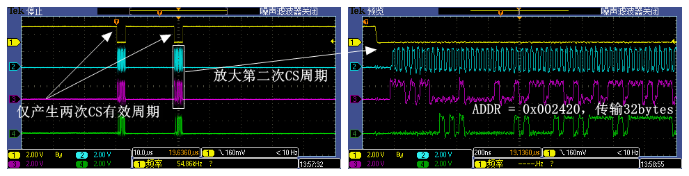
4.1.2 AHB_ADDR_START = 0x60002419
When the actual code reads Flash data that spans two adjacent 32-byte aligned data blocks (0x60002400 – 0x6000241f, 0x60002420 – 0x6000243f), the Flash end will show two valid CS signals, each transmitting 32 bytes of data, and D-Cache continues to operate. This time, two D-Cache Lines are utilized (the total size of D-Cache is 32KB, with 1024 Cache Lines), hence we still do not see periodic CS signals at the Flash end.
4.1.3 Additional Experiment: Reading 1KB from 0x60002400
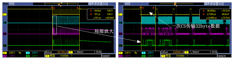
When the code loops to read 1KB of data, the waveform shows 32 valid CS signals, each transmitting 32 bytes of data, totaling 1KB of data transfer, and D-Cache sends out 32 Cache Lines. At the Flash end, we still do not see periodic CS signals.
4.2 Repeat the Experiments from the Prefetch Article
Now let’s repeat all experiments from the article “Actual Capture of Flash Signal Waveforms to Examine AHB Read Access Conditions Under the FlexSPI Peripheral of i.MXRT (With Prefetch)” with D-Cache enabled:
4.2.1 Loop to Read Any Length Data Block within 1KB Space Aligned to 32 Bytes, Starting Copy Address within the First 31 Bytes
In this case, the actual waveform at the Flash end is similar to the test results in 4.1 of the article “Actual Capture of Flash Signal Waveforms to Examine AHB Read Access Conditions Under the FlexSPI Peripheral of i.MXRT (With Prefetch)”; hence, no further images are shown. The Prefetch mechanism serves as the first layer of caching, while D-Cache retrieves results from the Prefetch Buffer as the second layer of caching. The only difference is that due to the presence of D-Cache, the starting cached address may change (from 8-byte alignment to 32-byte alignment):
#define PREFETCH_TEST_ALIGNMENT  (7) // Can take values 0 - 31
#define PREFETCH_TEST_START      (0x60002400 + PREFETCH_TEST_ALIGNMENT)
uint32_t testLen = 0x1;  // Can take values 1 - (1KB-PREFETCH_TEST_ALIGNMENT)
void test_cacheable_read(void)
{
    // Omit system configuration (I-Cache off, Prefetch on, D-Cache on)
    while (1)
    {
        memcpy((void *)0x20200000, (void *)PREFETCH_TEST_START, testLen);
    }
}
4.2.2 Loop to Read Data Blocks Greater than 1KB or 1KB Data Blocks with Non-32 Byte Aligned Starting Address
In this case, there will be two complete 1KB Prefetch operations at the Flash end. The first Prefetch operation reads 1KB from 0x60002400, and the second Prefetch operation reads 1KB from 0x60002800. Due to the presence of D-Cache, the second Prefetch operation has enough time to complete without needing to insert additional software delays to avoid being interrupted by the next access demand from the while(1) loop:
void test_cacheable_read(void)
{
    // Omit system configuration (I-Cache off, Prefetch on, D-Cache on)
    while (1)
    {
        memcpy((void *)0x20200001, (void *)0x60002401, 0x400);
    }
}
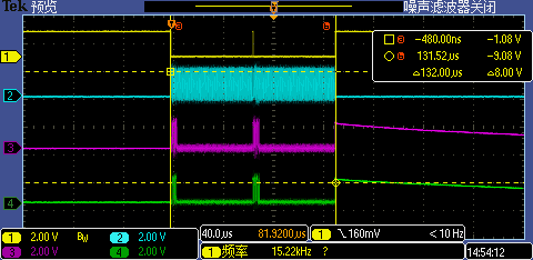
4.2.3 Loop to Read Two Different Data Blocks (Within Two Different 1KB Spaces Aligned to 32 Bytes)
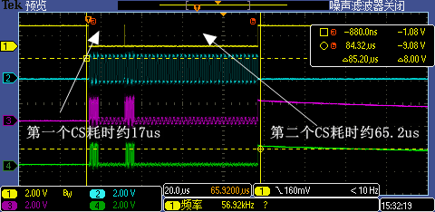
In this case, even with D-Cache present, the Prefetch operation during the first CS period (i.e., memcpy((void *)0x20200000, (void *)0x60002400, 0x100); triggered) is still interrupted by the Prefetch operation of the second CS (i.e., memcpy((void *)0x20200400, (void *)0x60002800, 0x100);). However, the Prefetch operation during the second CS period will not be interrupted since the next access demand from the while(1) loop has already been cached in D-Cache:
void test_cacheable_read(void)
{
    // Omit system configuration (I-Cache off, Prefetch on, D-Cache on)
    while (1)
    {
        memcpy((void *)0x20200000, (void *)0x60002400, 0x100);
        memcpy((void *)0x20200400, (void *)0x60002800, 0x100);
    }
}
4.3 How to See Periodic CS Signals with D-Cache Enabled
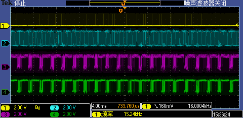
After testing so many situations, is it possible for us to see periodic CS signals at the Flash end, meaning that Flash is continuously being read? Of course, we can achieve this. We know that the total size of D-Cache is 32KB; as long as we loop to copy data exceeding 32KB, D-Cache will start to hold insufficient data. Below, the following code can allow us to see the long-lost periodic timing waveform (be careful, continuous work of Flash will consume more power, haha).
void test_cacheable_read(void)
{
    // Omit system configuration (I-Cache off, Prefetch on, D-Cache on)
    while (1)
    {
        memcpy((void *)0x20200000, (void *)0x60002400, (0x8000 + 1));
    }
}
Thus, the introduction of the actual capture of Flash signal waveforms to examine the AHB read access conditions under the FlexSPI peripheral of i.MXRT is complete. Where are the applause~~~

1. Foolproof tutorial: How to use the “All-in-One” development tool STM32CubeIDE
2. Microcontroller engineer looking to switch to embedded Linux after 6 years, not sure where to start?
3. Summary of 80 MCU manufacturers from China and abroad
4. Comparing STM32 and GD32 firmware libraries, you will discover the secrets within!
5. What is your microcontroller bare-metal program framework like?
6. Endorsement from the great Jim Keller! RISC-V is advancing into the AI and automotive chip fields!

Disclaimer: This article is a reprint from the internet, and the copyright belongs to the original author. If there are copyright issues, please contact us, and we will confirm the copyright based on the copyright certificate you provide and pay remuneration or delete the content.