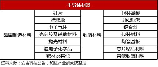
Semiconductor materials include wafer manufacturing materials and packaging materials. Wafer manufacturing materials include silicon wafers, mask plates, electronic gases, photoresists, CMP polishing materials, wet electronic chemicals, target materials, etc. Packaging materials include packaging substrates, lead frames, bonding wires, encapsulation materials, ceramic substrates, chip bonding materials, and other packaging materials.
Table 1-1 Classification of Semiconductor Materials
In the chip manufacturing process, silicon wafers are used in the silicon wafer stage; high-purity special gases and high-purity reagents are used in the cleaning stage; target materials are used in the deposition stage; photoresists are used in the coating stage; mask plates are used in the exposure stage; high-purity reagents are used in the development, etching, and stripping stages, and high-purity special gases are also used in the etching stage; precursors and target materials are used in the thin film growth stage; polishing liquids and polishing pads are used in the grinding and polishing stages. In the chip packaging process, packaging substrates and lead frames are used in the die bonding stage; bonding wires are used in the wire bonding stage; silica micro powder and molding materials are used in the molding stage; and tin balls are used in the electroplating stage.
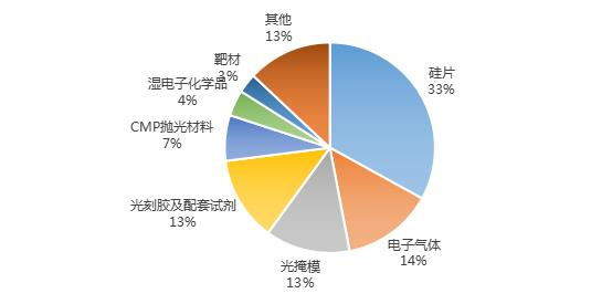
In terms of the composition of the semiconductor materials market, silicon wafers account for the largest share, at 33%. Electronic gases come second, with a share of 14%, while photomasks rank third, with a share of 13%. Additionally, photoresists and supporting reagents, CMP polishing materials, wet electronic chemicals, and target materials account for 13%, 7%, 4%, and 3%, respectively. Overall, the various segmented semiconductor materials markets are generally small.
Figure 1-1 Composition of the Semiconductor Materials Market
Data Source: China Business Industry Research Institute, He Da Industry Research Institute compilation
1. Overview of the Development of China’s Semiconductor Materials
Under the national policy guidance encouraging the localization of semiconductor materials, domestic semiconductor material manufacturers are continuously enhancing their technology levels and R&D capabilities, gradually breaking the monopoly of foreign semiconductor manufacturers, promoting the localization process of semiconductor materials in China, and facilitating the development of the semiconductor materials industry in China.
China is the largest semiconductor market globally, accounting for about 1/3. With the rapid development of the Chinese economy and the fast-paced promotion of consumer electronics such as mobile phones, PCs, and wearable devices, as well as emerging fields like new energy, the Internet of Things, and big data, the Chinese semiconductor market is rapidly growing.
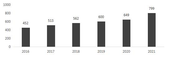
Data shows that from 2015 to 2021, the market size of semiconductor materials in China grew year by year, increasing from 45.2 billion yuan in 2016 to 79.9 billion yuan in 2021, with a compound annual growth rate of 12%.
Figure 2-1 Semiconductor Materials Market Composition (Unit: Billion Yuan)
Data Source: SEMI, He Da Industry Research Institute compilation
2. Overview of the Development of Sub-sectors of China’s Semiconductor Materials
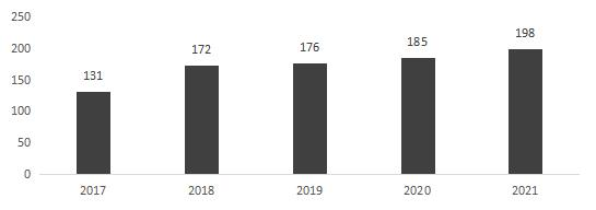
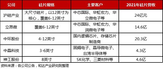
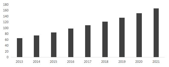
Silicon wafers are the semiconductor material with the highest value proportion. In recent years, the scale of China’s semiconductor silicon wafer market has shown a stable upward trend. According to statistics, the demand for semiconductor silicon wafers in China in 2021 was 19.8 billion yuan.
Figure 3-1 Market Size of China’s Semiconductor Silicon Wafers from 2017 to 2021 (Unit: Billion Yuan)
Data Source: IC Mtia, He Da Industry Research Institute compilation
Based on different sizes, silicon wafers can be classified as 50mm (2 inches), 75mm (3 inches), 100mm (4 inches), 150mm (6 inches), 200mm (8 inches), and 300mm (12 inches). The inch refers to the diameter of the silicon wafer, with 8-inch and 12-inch wafers being the most mainstream products in the market. 8-inch wafers are mainly used in processes of 90nm-0.25μm, predominantly for sensors, security fields, power devices in electric vehicles, analog ICs, fingerprint recognition, and display drivers. 12-inch wafers are primarily used in processes below 90nm, mainly for logic chips, memory devices, and autonomous driving fields.
The “large size” is the mainstream trend for silicon wafers. The larger the wafer, the more chips can be produced from a single wafer, leading to lower manufacturing costs; thus, wafer manufacturers are continuously moving towards larger-sized wafers. According to SEMI data, before 2008, the global large-sized wafer market was dominated by 8-inch wafers, but after 2008, the market share of 12-inch wafers gradually increased, surpassing that of 8-inch wafers. By 2020, the market share of 12-inch wafers had risen to 68.1%, making it the most mainstream product in the semiconductor silicon wafer market. Subsequently, 18-inch wafers are expected to become the next target in the market, but the difficulty of equipment development is high, production costs are high, and downstream demand is insufficient, so 18-inch wafers are not yet mature.
Table 3-1 Major Domestic Semiconductor Wafer Manufacturers and Project Progress
Electronic Specialty Gases Sector
From 2013 to 2020, the market size of electronic specialty gases in China grew from 6.48 billion yuan to 17.36 billion yuan, with a compound annual growth rate of 15.12%. In the future, with the expansion of downstream wafer plants and the accelerated localization of semiconductor materials, the domestic specialty gas market is expected to maintain a high growth trend.
Figure 3-2 Market Size of China’s Electronic Specialty Gases from 2017 to 2021 (Unit: Billion Yuan)
Data Source: China Semiconductor Industry Association, He Da Industry Research Institute compilation
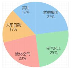
Electronic specialty gases have long been nearly monopolized by giants. In 2019, four giants—Air Products, Air Liquide, Taiyo Nippon Sanso, and Linde Group—divided 91% of the global market, indicating a clear oligopoly. The domestic market is no exception, with the four giants dominating 88% of the domestic share, and domestic manufacturers only occupying 12%. Moreover, for electronic specialty gases used in integrated circuit production, China can only produce 20% of the varieties, with the rest being highly dependent on foreign supply.
Figure 3-3 Structure of the Specialty Gas Market in China
Data Source: Jin Hong Gas Prospectus, He Da Industry Research Institute compilation
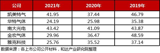
Specialty gas markets have high gross margins and strong profitability. Among all semiconductor material sectors, the average gross margin of electronic specialty gas companies is at a relatively high level. Comparing the semiconductor industry chain, wafer fabs have the strongest profitability; for example, the world’s largest wafer foundry, TSMC, has a gross margin of 51.6%, while the domestic leading wafer foundry, SMIC, has a gross margin of about 30%. For specialty gas companies, the average gross margin can reach nearly 50%. The second largest company in the world, Air Liquide, maintained a gross margin of 60%-65% from 2010 to 2019, while the gross margin of general chemical gases or bulk gases is only in the range of 20-30%. Domestic electronic specialty gas companies have relatively lower gross margins, around 25%-40%, compared to international giants, indicating ample future growth potential. With advancements in technology research and development and increasing demand, the profitability of electronic specialty gas manufacturers is expected to continue to upgrade.
Table 3-2 Comparison of Gross Margins of Major Domestic Electronic Specialty Gas Companies (%)
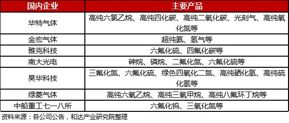
Table 3-3 Domestic Electronic Specialty Gas Product Landscape
Photomasks are the pattern masters used in the photolithography process of microelectronics manufacturing. The global photomask market for semiconductors continues to grow. According to SEMI data, the market size for photomasks used in semiconductor chips was 4.1 billion USD in 2019, and it is expected to reach 4.4 billion USD by 2022.
Benefiting from the rapid development of wafer manufacturing in mainland China over the past few years, the market size of semiconductor photomasks in mainland China has shown a rapid growth trend. The market size of semiconductor photomasks in China was 4.8 billion yuan in 2019, exceeding 6 billion yuan in 2021.
The photomask market is highly concentrated and is dominated by foreign companies. Photronics, Japan’s DNP, and Japan’s Toppan occupy more than 80% of the semiconductor photomask market share. The Chinese photomask industry can only meet the demand for mid-to-low-end products in the domestic market.
According to Omdia statistics, in the global sales ranking of photomask companies for flat panel displays, Qingyi Optoelectronics is the only Chinese company on the list, ranking fifth, while the others are Japanese, American, and Korean companies. In recent years, domestic companies have gradually narrowed the gap in market position with international competitors through continuous technology research and development and product upgrades.
Photoresists are the most important consumables in the photolithography process. Photoresists are photosensitive materials that undergo local solubility changes under specific light sources, mainly acting in the photolithography stage, and play a crucial role in transferring patterns from the mask onto the wafer.
During photolithography, a metal layer is applied to the silicon wafer, and the mask has a pre-designed circuit pattern. Light passes through the mask and illuminates the photoresist. If the photoresist exposed to ultraviolet light becomes soluble, the pattern on the mask is left after washing, this is called positive resist; conversely, it is called negative resist.
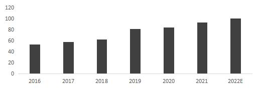
In recent years, the market size of photoresists in China has been steadily increasing, growing from 5.32 billion yuan in 2016 to 8.4 billion yuan in 2020, with an average compound annual growth rate of 12.1%, far exceeding the global industry growth rate. It is expected that the market size of photoresists in China will reach 10 billion yuan in 2022.
Figure 3-4 Market Size of Photoresists in China (Billion Yuan)
Data Source: Company announcements, He Da Industry Research Institute compilation
Despite the increasing demand for photoresists in the domestic market, China’s production capacity for panel photoresists remains severely insufficient. Currently, the production of panel photoresists is monopolized by Japanese and Korean manufacturers. For example, according to data from the Forward Industry Research Institute, Japanese, Korean, and Taiwanese companies such as Tokyo Ohka, LG Chem, Toyo Ink, Sumitomo Chemical, Mitsubishi Chemical, and Chi Mei occupy more than 90% of the market share, while China’s local supply capacity is relatively weak.
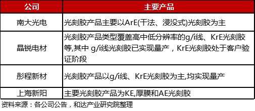
Currently, domestic companies engaged in the research and production of semiconductor photoresists include Jingrui Co., Nanda Optoelectronics, Shanghai Xinyang, and Beijing Kehua, mainly focusing on the production of i/g line photoresists, applied in integrated circuit processes above 350nm. In terms of KrF photoresists, Beijing Kehua and Xuzhou Bokan have achieved mass production. Nanda Optoelectronics has a relatively fast industrialization process for ArF photoresists, having undertaken the national 02 project for “Key Technology R&D Projects of High-Resolution Photoresists and Advanced Packaging Photoresists” and “Development and Industrialization Projects of ArF Photoresists.” It is also the first company to pass product verification of ArF photoresists by domestic customers, while other domestic companies are still in the research and verification stage.
Table 3-4 Major Domestic Semiconductor Photoresist Manufacturers
CMP systems’ main consumables are divided into polishing liquids and polishing pads, which account for 49% and 33% of the polishing material costs, respectively. Other polishing materials include polishing heads, grinding discs, testing equipment, cleaning equipment, etc.
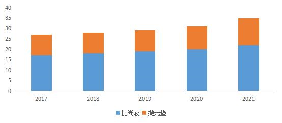
The high prosperity of the semiconductor industry drives stable growth in the CMP market. With the semiconductor materials industry’s upward trend, the CMP materials market is expected to maintain steady growth driven by the downstream market. In 2020, the global market sizes for polishing liquids and polishing pads were 1.34 and 0.82 billion USD, respectively. The market sizes for CMP materials in China in 2021 were 2.2 and 1.3 billion yuan, respectively. China is comprehensively developing the semiconductor materials industry, and the CMP polishing industry has broad growth potential in the future.
Figure 3-5 Market Size of CMP Materials in China (Billion Yuan)
Data Source: Huachuang Securities, He Da Industry Research Institute compilation
Formulating the right mixtures is a significant technical challenge. Due to the many applications of CMP polishing liquids, different customers have varying needs, requiring specific formulations that need to include oxidants, complexing agents, surfactants, corrosion inhibitors, and various other additives. Formulating suitable polishing liquid mixtures requires long-term technical accumulation and continuous R&D attempts by companies. Currently, many formulations are patented, creating high industry R&D barriers.
High trial-and-error costs and long certification times. Companies need to continuously find suitable formulations, stabilize manufacturing processes, and design patterns to achieve optimal and stable polishing rates and effects. Therefore, research on CMP materials is time-consuming, requiring a long time to explore the impacts of process parameters, product formulations, and other factors on physical parameters and performance, forming high industry know-how barriers.
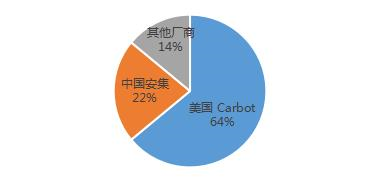
The global polishing liquid market is dominated by American Cabot, while domestic leader Anji Technology holds a market share of over 20%. Currently, the global polishing liquid market is mainly monopolized by American and Japanese manufacturers. American Cabot, American Versum, Japan’s Hitachi, Japan’s Fujimi, and American DuPont collectively hold nearly 80% of the global polishing liquid market share, while Anji Technology only accounts for about 3%. In the domestic market, American Cabot accounts for approximately 64%, while Anji Technology’s market share is 22%.
Figure 3-6 Market Share of Polishing Liquids in China
Data Source: Guanyan Tianxia, He Da Industry Research Institute compilation
Anji Technology is the leading domestic CMP polishing liquid manufacturer, with a market share exceeding 20%. The company has undertaken two “02 projects” from 2015 to 2016, focusing on continuously optimizing the stability of products above the 14nm technology node, testing and optimizing products for 14nm and below technology nodes, and developing polishing liquids for copper and copper barrier layers used in 128-layer and above 3D NAND and below 19/17nm technology nodes DRAM. Currently, the company has achieved large-scale production of CMP polishing liquids for the 13-14nm technology node, with downstream clients including major wafer manufacturers such as SMIC, Yangtze Memory Technologies, TSMC, and Hua Hong Semiconductor.
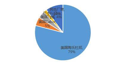
The global polishing pad market is “dominated by one player,” with domestic replacements steadily advancing. Currently, the global polishing pad market is mainly monopolized by American DuPont, with a market share of up to 79%, while other companies such as American Cabot, Japan’s Fujimi, and Japan’s Hitachi have market shares of less than 5%. Among domestic enterprises, Dinglong Co., Jiangfeng Electronics, and Wanhua Chemical have corresponding production capabilities. Among them, Dinglong Co. is the leading domestic polishing pad manufacturer, producing polishing pads aimed at competing with the American DuPont Group. With the expansion of domestic wafer manufacturers and increasing demand, domestic enterprises are welcoming a development boom.
Figure 3-7 Global Market Share of Polishing Pads
Data Source: Forward Industry Research Institute, He Da Industry Research Institute compilation
Dynamic | Wucheng Economic Development Zone: Seeking “Development Increment” from “Land Stock” to Promote Quality and Efficiency of Enterprises
Dynamic | “Five Certificates Issued Together” within 24 Hours! Geely Tonglu Power Battery Project Launched!
Dynamic | The Changbai Mountain-Hangzhou Cooperation and Investment Promotion Conference Held in Hangzhou
✎Source | He Da Industry Research Institute Author: Jing Weicai
✎Editor | Shen Han
✎Review | Wang Wanjun
Welcome to Share in Moments
Please leave a message for cooperation contact