In the previous article “Chip Journey (4) – Introduction to Tapeout Design”, the design company and foundry have communicated the tapeout requirements through specified channels. This article begins to introduce the tapeout process for chips, which is also the start of another costly phase of the project.For the fab, the tapeout process generally includes the following steps: different fabs may have slight variations depending on their process nodes.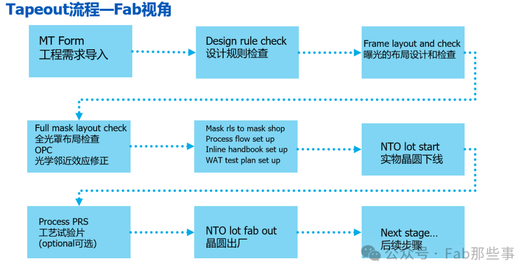 1. Importing Engineering RequirementsPlease refer to “Chip Journey (4) – Introduction to Tapeout Design”, which mainly involves transmitting engineering requirements through fixed channels.2. Design Rule CheckAfter the design house completes the design, it will use the design rule algorithms provided by the fab to check its own design. If any design rules are violated, modifications will be made. Additionally, some special designs that cannot be modified may be allowed to pass, but documentation must be generated to clearly communicate with the fab.When the fab receives the client’s GDS file, it will also perform a design rule check. Similarly, any non-compliant items need to be aligned with the design side, choosing to either return for modification or evaluate and allow to pass.3. Frame Layout and CheckThe frame, as the name suggests, is the framework. Generally, the design house designs the layout of the main chip. The fab needs to design the exposure shots, which include the design of the cutting paths, typically containing:1) Photolithography alignment/registration marks,2) WAT test patterns,3) Critical dimension (CD)/thickness (THK) measurement patterns,4) Other patterns, such as reliability test patterns, etc.The following image shows some typical components of cutting paths (please note the different colors representing different functions):
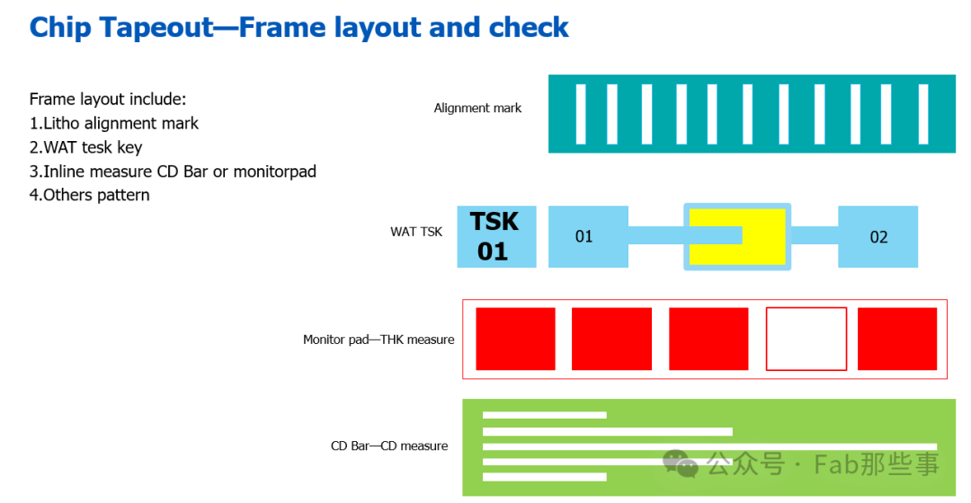 With the different functional components of the cutting paths, they need to be arranged according to the product.This introduces the concept of a shot, which we typically define as the area of a photomask that can be exposed in one exposure. A shot usually contains at least one die, and one exposure may encompass several die areas.
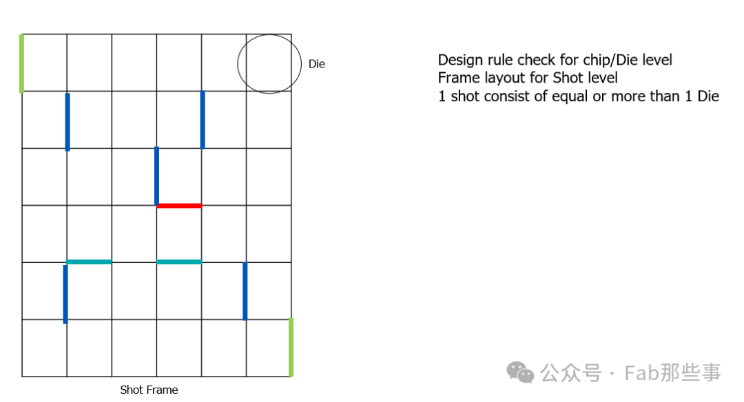 The image shows a basic shot, with the black lines representing the cutting paths, where various functional patterns are placed. Once completed, a frame file is generated.4. Full Photomask Layout Check
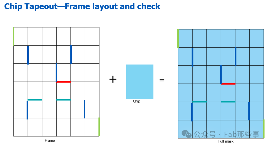 The full photomask layout is the overlay of the frame layout file and the chip layout, forming the entire photomask pattern. At this stage, the global photomask is basically finalized, requiring PIE/Tapeout checks to ensure the layout is correct, that no necessary test structures are missing, and that there are no misalignments between layers.After completing the full photomask check, optical proximity correction (OPC) is performed to correct optical proximity effects. Once corrected, it can be sent to the photomask factory for photomask production.The following image shows a physical photomask, which is generally made from quartz.The photomask reflects a shot (the basic unit of one exposure),and outside the exposure area of the photomask, it will include:1) The photomask identification code, defining which product it is used for, as well as which layer and version, to prevent confusion when retrieving the photomask.2) The alignment marks on the photomask, used during alignment in the photolithography machine.
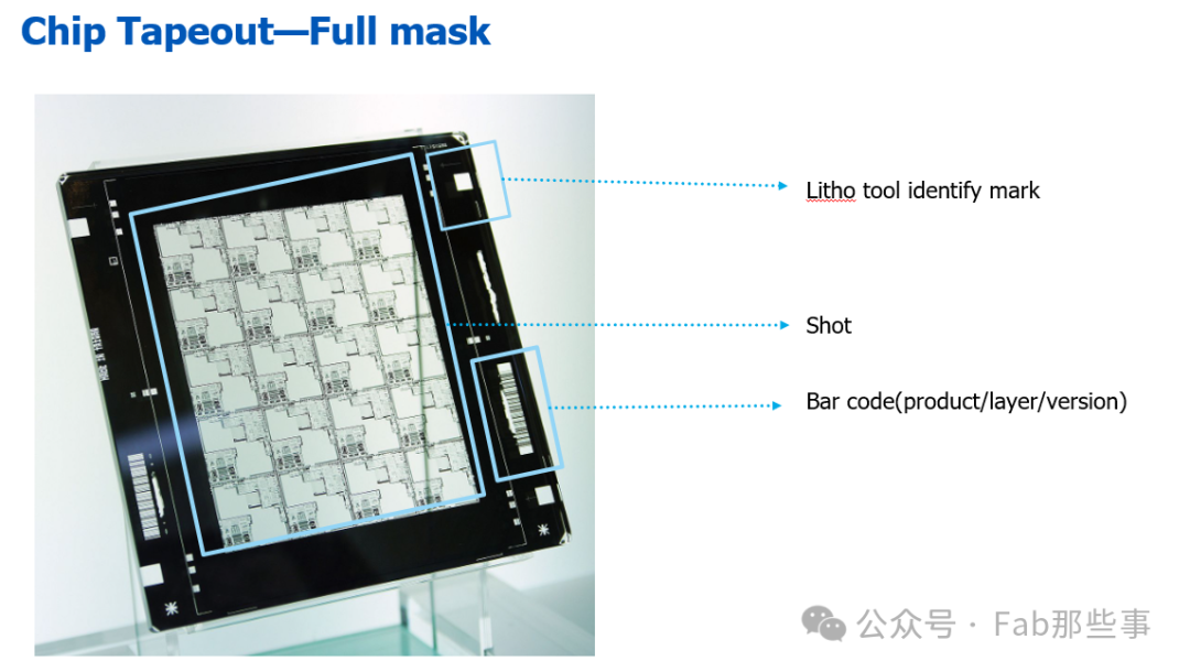 As a side note, the price of a single wafer during the tapeout phase is significantly higher than during mass production.As process nodes advance, the costs continue to rise.Thus, the tapeout phase is a major hurdle for design companies, and many design houses struggle to secure funding for two tapeouts; cases of companies dissolving after a single unsuccessful tapeout are common.Therefore, the tapeout phase is a significant financial burden in physical manufacturing.5. Tapeout PreparationWhile sending the work order to the photomask factory for photomask production, the fab’s internal tapeout preparations will also begin in parallel.The fab needs to prepare the following tasks:1. Process Flow SetupThe flow needs to utilize the product’s reference baseline flow, corresponding control plans, and MT Form (special requirements).The process flow is set up by PIE according to the client’s engineering requirements, including the number of layers, devices used, and special requirements, to jointly generate the flow file, which is activated under BR’s operation.For more details, please refer to“Fab Beginner’s Guide – What is Flow”2. Measurement Manual CompilationDuring the chip production process, various processes and structures need to be measured to ensure quality and stability, which requires compiling the corresponding measurement manual. After inspection by PIE, the measurement manual is submitted to the MMT measurement engineer, who will create the corresponding measurement process program, also known as a recipe, on the measurement equipment after the new product is offline.The measurement manual includes:1) Layer information,2) Measurement position coordinates in the shot,3) Theoretical reference values for data result verification,4) Shot positions measured on the wafer,5) Types of measurement data, such as CD critical dimensions/THK thickness/AFM step height, etc.3. WAT Test Plan CompilationSimilar to the measurement manual, the WAT test plan includes the following content:1) Test items,2) Test locations,3) Test methods/test conditions, such as how to apply voltage and to what extent, conditions for reading values, etc.4) Target values and limits for testing.The following image is a schematic of WAT Testkeys, where each TSK contains many test structures placed in the cutting paths, with test structures having external test probe pins, represented by the bright yellow squares, also known as metal pads.
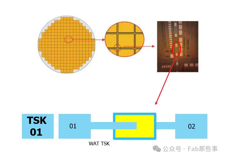 4. Process Experiment Plan DevelopmentIn many cases, the designs from design companies may involve new structures or processes, which will require arranging experiments to first conduct preliminary assessments. Once the experimental conditions are identified in the test chips, the design house’s NTO products can smoothly pass through when they arrive, saving production time and shortening the tapeout cycle.This phase requires confirmation and collaboration from the fab PIE/PE and design house PDE to jointly propose and develop the experimental plan. Sometimes, due to schedule requirements, MFG assistance is also needed.6. Start of TapeoutOnce the photomask arrives at the factory and preliminary work is completed, the tapeout officially begins. To minimize the tapeout cycle, the NTO lot process requires the responsible PIE to be fully committed, maintaining a 24-hour on-call status. Any data anomalies during tapeout need to be responded to promptly.For measurement data during production, it should be checked as early as possible to confirm whether it is in a normal state. If anomalies occur, they need to be addressed quickly. If there are results that cannot be changed or remedied, a new tapeout will be required, which can impact the client’s schedule and may affect the fab’s professionalism in the client’s eyes.Upon completion of the tapeout, the PIE needs to confirm whether the WAT electrical parameters are normal. If they are, the products can be shipped out, allowing the design company to continue with functional verification, yield testing, final yield testing after packaging, and reliability testing of the product.7. Wafer Shipment from TapeoutAfter the wafer is shipped out from the fab, the fab’s work temporarily concludes, awaiting the design company’s verification results. If the verification results are all normal, consideration will be given to transitioning to mass production.If the verification results are abnormal, a joint study of solutions and improvement plans will be necessary to continue advancing the project towards mass production.This issue briefly introduced the wafer tapeout process, and the next issue will continue to explore backend packaging and testing.Comments and discussions are welcome.