We take photos with our smartphones every day, capturing moments of our lives. However, you may not know that the raw data collected from the CMOS sensor at the moment the shutter is pressed is often filled with “flaws.” So why do the final images look so clean? This is thanks to a behind-the-scenes hero—the Image Signal Processor (ISP)—and its crucial internal “repair magic”: bad pixel correction algorithm.
1
The Source of the Problem: “Flaws” on the CMOS Sensor
First, we need to understand where the problem originates. The core of the camera is the CMOS image sensor, which you can think of as a massive grid composed of millions or even billions of pixels. Each pixel is responsible for receiving light and converting it into an electrical signal.
However, while a perfect CMOS chip theoretically exists, it is very difficult to achieve in reality. Due to microscopic differences in the manufacturing process, long-term use, or high-temperature and high-humidity environments, some pixels inevitably become “unruly”:
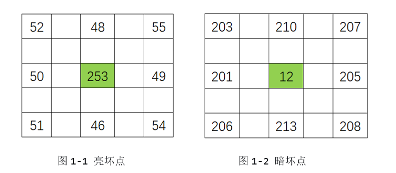
Bright Bad Pixels: They act like an “overzealous employee,” continuously outputting an abnormally high signal even in complete darkness, resulting in a permanent bright spot or color blotch in the final photo.
Dark Bad Pixels: In contrast, these pixels are completely “on strike,” always outputting black regardless of the light intensity.
If these flaws are not addressed, they will permanently mar every photo, much like an ink stain on a white shirt. The ISP’s bad pixel correction algorithm is designed to automatically fix these ink stains.
2
The Foundation of the Algorithm: Static Bad Pixel Correction and the “Bad Pixel Map”
This is the most basic and core correction method, akin to a teacher managing students with a “watch list.” It consists of two phases:
Phase One: Establishing a “Blacklist”—The Bad Pixel Map
This process is usually completed before the phone leaves the factory or when the camera is powered on. The system prompts the sensor to take a quick shot in complete darkness (with the lens cap on).
Algorithm Logic: In the absence of light, normal pixels will only output a very low and uniform random noise (background noise). Bad pixels will “stand out,” outputting an abnormally high signal far above the average level.
Execution Process: The ISP scans the raw image output from the entire sensor and uses a threshold judgment algorithm to record the coordinates (e.g., row X, column Y) of all pixels whose output signal exceeds a predetermined threshold, generating a bad pixel map that is permanently stored in the device’s memory.
Phase Two: Real-Time Repair—The “Neighborhood Interpolation” Algorithm
When users take photos normally, the ISP will refer to this “bad pixel map” in real-time. For each bad pixel marked on the map, the ISP will never use the erroneous data it provides. So what will it use instead? The answer is:to seek help from its neighbors.
The most commonly used and efficient algorithm is the median filtering algorithm.
How does it work? Imagine a bad pixel sitting in the center of a 3×3 grid. The ISP will immediately gather the brightness values of the surrounding 8 “neighbor” pixels.
1.Collect: Read the values of the surrounding 8 pixels.
2.Sort: Sort these 8 values from low to high.
3.Take the Median: Take the value that is in the middle after sorting (the 4th or 5th largest value) as the final result.
4.Replace: Replace the bad pixel’s original anomalous value with this median value.
Why use the “Median” instead of the “Average”?
Because the average can easily be skewed by another noise point that may exist among the neighbors. The median has excellent resistance to impulse interference, ensuring that the replacement value best represents the true background of the area, making the transition after repair very natural and leaving no trace of the fix.
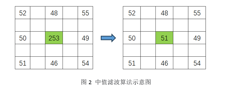
For example, the process of repairing a bright bad pixel. In a 3×3 pixel grid, the center is marked as a “bad pixel” with a value of 253 (abnormally high). The surrounding 8 pixels are normal, with values of 52, 48, 55, 50, 49, 51, 46, 54.
Algorithm Steps:
1. Sorted as follows:
46,48,49,50,51,52,54,55,253;
2. Median → 51;
3. Replacement → The bad pixel value changes from 253 to 51.
3
The Evolution of the Algorithm: Dynamic Bad Pixel Correction
Static correction is very effective, but CMOS sensors may temporarily produce new “dynamic bad pixels” under high temperatures or prolonged exposure. Advanced ISPs have developed smarter dynamic bad pixel correction algorithms.
This algorithm no longer relies on a fixed “blacklist” but performs real-time analysis on each frame of the image. Its core idea is:
Adaptive Threshold Judgment: The ISP analyzes the local statistical characteristics of the current scene. If a pixel’s value significantly deviates from its surrounding pixels (in brightness and color) beyond a dynamically calculated threshold based on the current scene, it will be immediately flagged as a suspicious bad pixel and repaired using the neighborhood interpolation algorithm.
This is akin to a teacher not just looking at the list but continuously observing all students’ performances. Once someone exhibits abnormal behavior, immediate intervention occurs. This allows the camera to maintain image purity in various complex environments.
Conclusion
The bad pixel correction algorithm in ISPs is a silent yet remarkable achievement in modern imaging technology. It operates behind the CMOS sensor, functioning within milliseconds to silently erase flaws from every photo. Haitusense Microelectronics has independently developed the dynamic bad pixel correction algorithm, continuously optimizing area and power consumption, and has successfully applied it across various product lines.

Official Website
www.haitusense.com
National Service Phone
0551-63630677
Official Email
★
Company Profile
★
Hefei Haitusense Microelectronics Co., Ltd. is a semiconductor technology enterprise specializing in the research, design, and sales of high-performance CMOS image sensors, strategically invested by the well-known Anhui-based enterprise group—Fuhuang Group, which has over thirty years of development history, in collaboration with industry professionals from home and abroad.
The company has a complete CIS product R&D team, covering key positions such as pixel, ADC, circuit, process integration, and testing, with over 60% of R&D personnel. With Hefei as the R&D headquarters, it has established R&D centers in Shanghai and Japan, and regional branches in Beijing and Shenzhen, focusing on practicality and efficiency.
In today’s rapidly changing industrial environment, as a CIS design company, Haitusense Microelectronics collaborates with rapidly growing domestic wafer manufacturers to promote technological advancements in the CIS process platform. Its products are widely used in industrial inspection, intelligent transportation, machine vision, scientific instruments, automotive electronics, security, and other fields, dedicated to breakthroughs and innovations in advanced imaging technology and core components.
As a core member of the intelligent new vision industry segment of Fuhuang Group, Haitusense Microelectronics adheres to the core value of “first being a person, then being a business” and has been committed to the mission of “core technology leading visual perception technology” since its establishment, continuously providing better services to customers and sharing technological innovation achievements, fostering mutual growth!

Note: Some images are sourced from the internet.