Introduction
The electrical connections between various components on FR4 copper-clad PCBA are achieved through the copper foil traces and vias on its layers.
Due to the varying current levels in different products and modules, designers need to know whether the designed traces and vias can carry the corresponding current to fulfill the product’s functionality and prevent damage from overcurrent. This article introduces the design and testing methods for the current carrying capacity of traces and vias on FR4 copper-clad boards, and the test results can provide references for designers in future designs, making PCB design more reasonable and compliant with current requirements.Introduction Currently, the main material for printed circuit boards (PCBs) is FR4 copper-clad laminate, with copper foil of at least 99.8% purity providing electrical connections between components on the plane, while plated through holes (i.e., vias) achieve electrical connections between copper foils of the same signal in space. However, the design of copper foil width and the definition of via diameter have traditionally relied on experience. To make layout designs more reasonable and meet requirements, tests on the current carrying capacity of copper foils with different wire diameters were conducted, using the test results as a reference for design.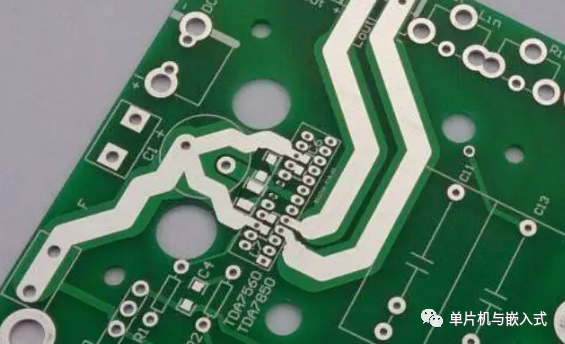 Factors Affecting Current Carrying Capacity Different module functions in PCBA products have varying current levels, so we need to consider whether the traces, which act as bridges, can carry the current flowing through them. The main factors determining current carrying capacity are: Copper foil thickness, trace width, temperature rise, and via diameter. In actual design, factors such as product usage environment, PCB manufacturing process, and material quality must also be considered.1 Copper Foil Thickness In the early stages of product development, the copper foil thickness of the PCB is defined based on product cost and the current state of the product. Generally, for products without high current, a copper foil thickness of about 17.5μm for outer (inner) layers can be selected:
- If the product has some high current, and the board size is sufficient, a copper foil thickness of about 35μm for outer (inner) layers can be selected;
- If most signals in the product are high current, a copper foil thickness of about 70μm for inner layers must be selected.
For PCBs with more than two layers, if the outer and inner layer copper foils are of the same thickness, the current carrying capacity of traces with the same wire diameter will be greater for the outer layer than for the inner layer.
For example, if both the inner and outer layers use 35μm copper foil: after etching the inner layer traces, lamination is performed, so the inner layer copper foil thickness is 35μm. After etching the outer layer traces, drilling is required. Since the holes do not have electrical connectivity after drilling, chemical copper plating is needed. This process involves plating copper on the entire board, so the outer layer copper foil will receive a certain thickness of copper, generally between 25μm and 35μm, resulting in an actual outer layer copper foil thickness of approximately 52.5μm to 70μm. The capabilities of copper foil suppliers vary, and the uniformity of copper foil may differ, but the differences are negligible, so the impact on current carrying capacity can be ignored.2 Trace Width Once the copper foil thickness is selected for the product, the trace width becomes a decisive factor for current carrying capacity. The design value of trace width and the actual value after etching may have some deviation, generally allowing a deviation of +10μm/-60μm. Since traces are formed by etching, there may be residual etching solution at the corners of the traces, making the corners generally the weakest points. Therefore, when calculating the current carrying capacity of traces with corners, the value measured on straight traces should be multiplied by (W-0.06)/W (where W is the trace width in mm). 3 Temperature Rise Continuous current flowing through PCB traces will cause the traces to heat up, leading to a sustained temperature rise. When the temperature rises to the substrate’s TG temperature or exceeds it, it may cause the substrate to warp, bubble, or deform, affecting the bonding strength between the trace copper foil and the substrate, leading to trace warping and breakage.
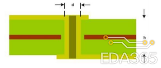
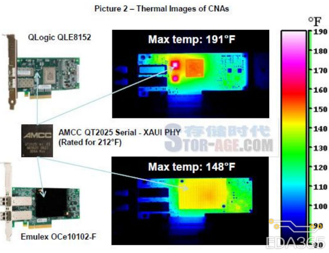 When a transient high current flows through PCB traces, the weakest points of the copper foil traces may not be able to dissipate heat to the environment quickly enough, resembling an adiabatic system, causing the temperature to rise sharply to the melting point of copper, burning the copper traces.4 Via Diameter Vias achieve electrical connections between different layers through copper plating on the via walls. Since the entire board is copper plated, the copper thickness on the walls of vias with different diameters is the same. The current carrying capacity of different diameter vias depends on the circumference of the copper wall.
 Testing PCB Design Currently, the TG temperatures used are >135℃ and >150℃ for substrates. Considering ROHS requirements for lead-free materials, PCBs will gradually switch to lead-free, necessitating the selection of substrates with TG temperatures >150℃. Therefore, the substrate for this test board is Shengyi S1000. The test board PCB size is 164mm wide and 273.3mm long. The PCB is manufactured by Shenzhen Mutai Technology Co., Ltd. The test board PCB is divided into three groups.1 First Group: The outer layer copper foil is 17.5μm, and the inner layer copper foil is 35μm. The first group test board PCB uses outer layer 17.5μm base copper and inner layer 35μm base copper. The outer layer wire diameters are:0.125mm, 0.16mm, 0.2mm, 0.25mm, 0.3mm, 0.4mm, 0.5mm, 0.6mm, 0.7mm, 0.8mm, 0.9mm, 1.0mm, 1.2mm, 1.5mm, 2.0mm, 2.4mm, 2.8mm, 3.0mm, 3.5mm, 4.0mm, 4.5mm, 5.0mm, 5.5mm, 6.0mm, 6.5mm, 7.0mm, 7.5mm, 8.0mm. Two samples for each wire diameter. The inner layer wire diameters are:0.125mm, 0.16mm, 0.2mm, 0.25mm, 0.3mm, 0.4mm, 0.5mm, 0.6mm, 0.7mm, 0.8mm, 0.9mm, 1.0mm, 1.2mm, 1.5mm, 2.0mm, 2.4mm, 2.8mm, 3.0mm, 3.5mm, 4.0mm, 4.5mm, 5.0mm, 5.5mm, 6.0mm, 6.5mm, 7.0mm, 7.5mm, 8.0mm. Two samples for each wire diameter. The via diameters are:0.15mm, 0.25mm, 0.3mm, 0.5mm, 0.7mm. Two samples for each via diameter.2 Second Group: The outer layer copper foil is 35μm, and the inner layer copper foil is 70μm. The second group test board PCB uses outer layer 35μm base copper and inner layer 70μm base copper. The outer layer wire diameters are:0.125mm, 0.16mm, 0.2mm, 0.25mm, 0.3mm, 0.4mm, 0.5mm, 0.6mm, 0.7mm, 0.8mm, 0.9mm, 1.0mm, 1.2mm, 1.5mm, 2.0mm, 2.4mm, 2.8mm, 3.0mm, 3.5mm, 4.0mm, 4.5mm, 5.0mm, 5.5mm, 6.0mm, 6.5mm, 7.0mm, 7.5mm, 8.0mm. Two samples for each wire diameter. For the 70μm copper foil thickness, the current suppliers’ capability allows for a minimum inner layer wire diameter of 0.2mm, so the inner layer wire diameters are:0.2mm, 0.25mm, 0.3mm, 0.4mm, 0.5mm, 0.6mm, 0.7mm, 0.8mm, 0.9mm, 1.0mm, 1.2mm, 1.5mm, 2.0mm, 2.4mm, 2.8mm, 3.0mm, 3.5mm, 4.0mm, 4.5mm, 5.0mm, 5.5mm, 6.0mm, 6.5mm, 7.0mm, 7.5mm, 8.0mm. Two samples for each wire diameter. The via diameters are:0.15mm, 0.25mm, 0.3mm, 0.5mm, 0.7mm. Two samples for each via diameter.3 Third Group: The outer layer copper foil is 70μm, and the inner layer copper foil is 105μm. The third group test board PCB uses outer layer 70μm base copper and inner layer 105μm base copper. For the 70μm copper foil thickness, the current suppliers’ capability allows for a minimum outer layer wire diameter of 0.3mm, so the outer layer wire diameters are:0.3mm, 0.4mm, 0.5mm, 0.6mm, 0.7mm, 0.8mm, 0.9mm, 1.0mm, 1.2mm, 1.5mm, 2.0mm, 2.4mm, 2.8mm, 3.0mm, 3.5mm, 4.0mm, 4.5mm, 5.0mm, 5.5mm, 6.0mm, 6.5mm, 7.0mm, 7.5mm, 8.0mm. Two samples for each wire diameter. For the 105μm copper foil thickness, the current suppliers’ capability allows for a minimum inner layer wire diameter of 0.3mm, so the inner layer wire diameters are:0.3mm, 0.4mm, 0.5mm, 0.6mm, 0.7mm, 0.8mm, 0.9mm, 1.0mm, 1.2mm, 1.5mm, 2.0mm, 2.4mm, 2.8mm, 3.0mm, 3.5mm, 4.0mm, 4.5mm, 5.0mm, 5.5mm, 6.0mm, 6.5mm, 7.0mm, 7.5mm, 8.0mm. Two samples for each wire diameter. The via diameters are:0.15mm, 0.25mm, 0.3mm, 0.5mm, 0.7mm. Two samples for each via diameter.Testing Plan Based on IPC-TM-650 TEST METHODS MANUAL section 2.5.4 on multilayer boards’ current carrying capacity, the testing plan is designed as follows. At room temperature, for testing inner and outer layer traces: a temperature sensor is attached to the middle position of the copper foil trace to be tested, and current is applied at both ends of the copper foil trace. After the temperature rise ΔT stabilizes, it is maintained for 3 minutes, and ΔT is recorded. The current is gradually increased until the copper foil trace is destroyed. At room temperature, for testing vias: a temperature sensor is attached to the VIA, and current is applied at both ends of the trace leading out from the VIA. After the temperature rise ΔT stabilizes, it is maintained for 3 minutes, and ΔT is recorded. The current is gradually increased until the VIA is destroyed. The current range is 0~100A. Sample values:0.1A, 0.2A, 0.3A, 0.4A, 0.5A, 0.6A, 0.7A, 0.8A, 0.9A, 1A, 1.2A, 1.5A, 1.8A, 2A, 2.3A, 2.5A, 2.7A, 3A, 4A, 5A, 6A, 7A, 8A, 9A, 10A, 15A, 20A, 25A, 30A, 35A, 40A, 45A, 50A, 55A, 60A, 65A, 70A, 75A, 80A, 85A, 90A, 95A, 100A.Analysis of Test Results Here, only the analysis of the first group of test data results is presented.1 Analysis of Wire Diameter Test Results Taking the outer layer copper foil with a wire diameter of 2.8mm as an example, the measured data is shown in Table 1.
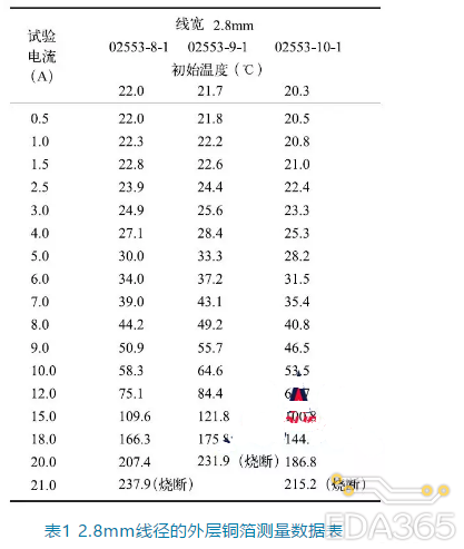 Based on the measured data in Table 1, a trend chart can be created, as shown in Figure 1:
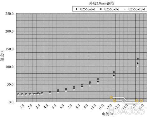 Figure 1: Temperature Rise and Current Trend for 2.8mm Outer Layer Copper Foil Wire Diameter From the average values of the measured data, we can conclude that the 2.8mm outer layer copper foil trace can carry approximately 8A of current at a temperature rise of ΔT=20℃; approximately 10.8A at ΔT=40℃; approximately 13A at ΔT=60℃; approximately 16A at ΔT=100℃; and the maximum continuous current capacity is approximately 20A. Using the above method, we can obtain the current carrying capacity of different wire diameters for 17.5μm outer layer copper foil and 35μm inner layer copper foil.2 Analysis of Via Test Results Since temperature measurement for vias cannot be performed on the copper layer of the via walls, we measure the temperature on the via pad surface, so the following test data is for reference only.
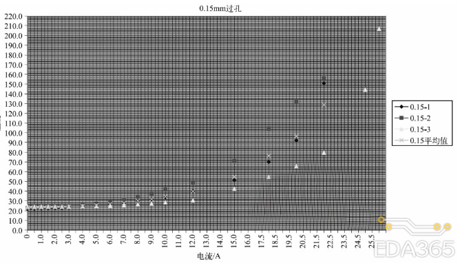 Figure 2: Temperature Rise and Current Trend for 0.15mm Via Diameter The measurement values for vias with diameters of 0.25mm, 0.3mm, 0.5mm, and 0.7mm are omitted here, but can be summarized in Table 2.
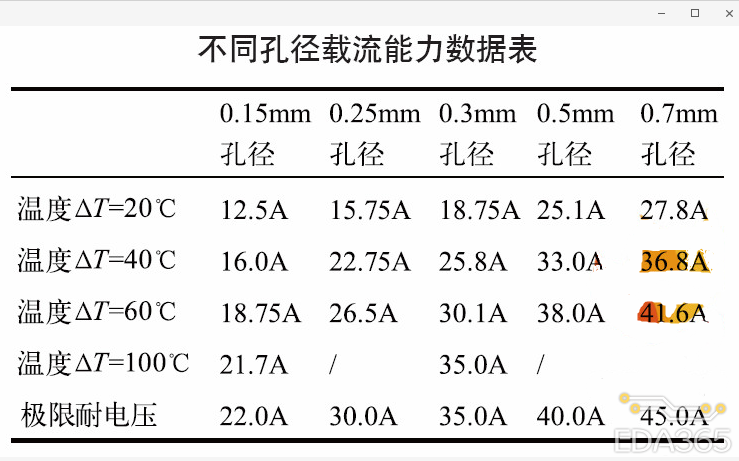 Table 2: Current Carrying Capacity Data for Different Via Diameters on 17.5μm Outer Layer / 35μm Inner Layer Copper Foil PCBConclusion Through this experiment and the analysis of experimental data, we have gained a relatively intuitive understanding of the current carrying capacity of traces and vias on copper-clad PCBs. However, on one hand, the test board was not produced by a mass production supplier, and the differences in manufacturing processes affect the variations in trace width and via wall thickness and circumference; on the other hand, there are certain differences in the heat dissipation conditions of each sample during the experiment. Additionally, the design of the test board and the experimental plan are idealized, while the actual product’s installation position, component distribution, wiring density, and the materials used are all factors that the test board cannot simulate, so the analysis data cannot directly guide design. However, in future development and design, we can refer to the data from this experiment. We can also adjust the experimental data based on design situations and practical verification in future products to provide more accurate guidance for design.