Typically, the current design for PCBs does not exceed 10A, especially in home and consumer electronics, where the continuous working current on a PCB usually does not exceed 2A.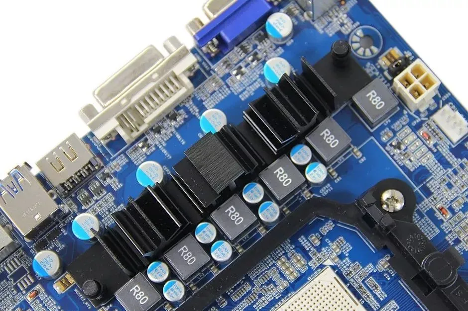 However, some product designs for power traces can sustain continuous currents of around 80A. Considering instantaneous currents and leaving a margin for the entire system, the continuous current for power traces should be able to withstand over 100A.So the question arises, what kind of PCB can withstand 100A of current?Method 1: Traces on the PCBTo understand the overcurrent capacity of a PCB, we first need to look at the structure of the PCB. Taking a double-sided PCB as an example, this type of circuit board usually has a three-layer structure: copper foil, substrate, and copper foil. The copper foil is the path through which current and signals pass in the PCB.According to basic physics knowledge, the resistance of an object is related to the material, cross-sectional area, and length. Since our current flows through the copper foil, the resistivity is fixed. The cross-sectional area can be considered as the thickness of the copper foil, which is the copper thickness in the PCB processing options.Typically, copper thickness is expressed in OZ; 1 OZ of copper thickness converts to 35 um, 2 OZ is 70 um, and so on. Thus, we can easily conclude that when passing large currents through a PCB, the traces should be short and wide, and the thicker the copper, the better.In practice, there is no strict standard for the length of traces. Engineering typically uses three indicators: copper thickness/temperature rise/wire diameter to measure the current-carrying capacity of the PCB.The following two tables can be referenced:
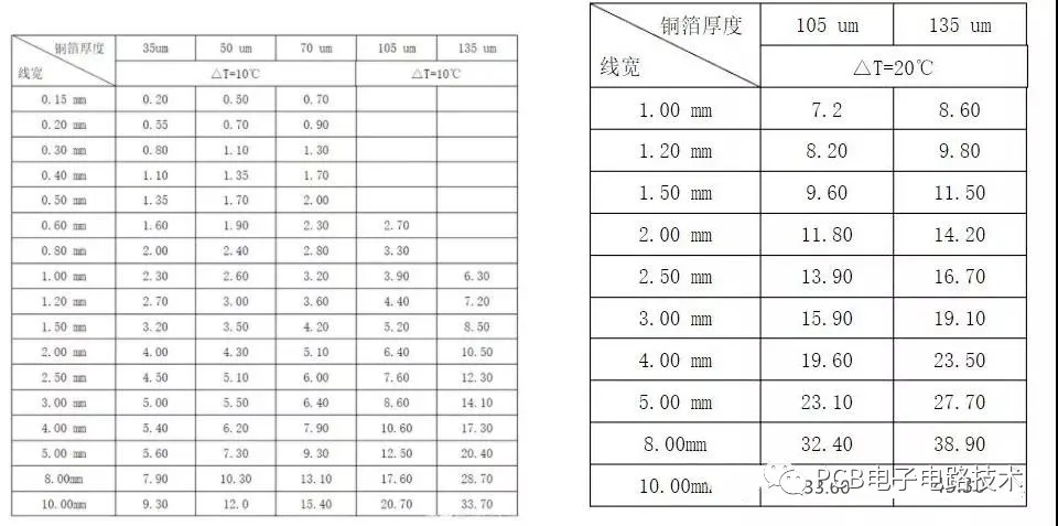 From the tables, we can roughly see that a 1 OZ copper thickness PCB can carry a current of 4.5 A with a wire width of 100 mil (2.5 mm) at a temperature rise of 10°.Moreover, as the width increases, the PCB’s current-carrying capacity does not strictly increase linearly; instead, the rate of increase gradually diminishes, which is consistent with practical engineering situations. If the temperature rise is increased, the wire’s current-carrying capacity can also be improved.Based on these two tables, the PCB wiring experience can be summarized as: increasing copper thickness, widening wire diameter, and enhancing PCB heat dissipation can improve the PCB’s current-carrying capacity.So if I need to carry 100 A of current, I can choose a copper thickness of 4 OZ, set the trace width to 15 mm, use double-sided traces, and add heat dissipation devices to lower the temperature rise of the PCB and improve stability.Method 2: Terminal BlocksIn addition to routing on the PCB, terminal blocks can also be used for wiring.
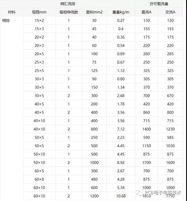 Fix several terminal blocks that can withstand 100 A, such as surface-mounted nuts, PCB terminal blocks, copper posts, etc., on the PCB or product casing.Then use terminals like copper lugs to connect wires that can carry 100 A to the terminal blocks. This way, large currents can be routed through the wires.Method 3: Custom Copper BusbarsAdditionally, custom copper busbars can be made. Using busbars to carry large currents is a common practice in industry, such as in transformers, server cabinets, and other applications that use busbars to carry large currents.Disclaimer:All rights to this article belong to the original author and do not represent the views of the association.The articles promoted by the “Jiangxi Province Electronic Circuit Industry Association” are for sharing purposes only and do not represent the position of this account. If there are copyright issues, please contact us for deletion.