The Relationship Between SPI Mold Polishing Grades and 3D Mold Polishing Grades

The Relationship Between SPI Mold Polishing Grades and 3D Mold Polishing Grades

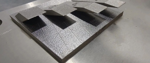
The following diagram shows the SPI standard mold polishing grade table, from which the polishing grades A~D in the mold industry originate. The A-grade claimed by 3D mold manufacturers also comes from here. There are four columns: ~ The first column is the grade code ~ The second column is the abrasive, tool, and polishing … Read more
Comparison of SPI, DSPI, and QSPI Technologies

Comparison of SPI, DSPI, and QSPI Technologies

Click the aboveblue text to follow us In embedded systems, the Serial Peripheral Interface (SPI) and its extensions (such as DSPI and QSPI) are widely used for high-speed communication with external devices (such as sensors, memory, LCD controllers, etc.). The main differences are as follows: 1 SPI SPI (Serial Peripheral Interface) is a full-duplex synchronous … Read more

A Brief History of the Development of Embedded Devices and Microcomputers

A Brief History of the Development of Embedded Devices and Microcomputers

Did you know? The smartphones, smartwatches, washing machines, and even cars we use every day all contain an “invisible brain”—the embedded system. The microcomputers that allow developers to easily create various smart gadgets are quietly changing the world. This all began over 60 years ago. In the 1960s, the prototype of embedded systems appeared in … Read more

Cutting-Edge Technology: A 9 cm, 25 g Miniature Wireless Amphibious Robot!

  The actuator is a device with controllable deformation capabilities and is considered the “heart” of miniature robots. A research team from Tsinghua University has recently developed a film-like miniature actuator that allows miniature robots to achieve continuous shape changes and “lock” specific action forms, enhancing their adaptability to various environments. The researchers stated that using … Read more

Assistance with 1.4nm Chip Flexible Substrate Technology

Assistance with 1.4nm Chip Flexible Substrate Technology

1.4nm ChipFlexible Substrate 1. SiO₂ nanoparticle doping rate (5-20wt%) 2. Nanocellulose diameter (10-15nm) 3. Metal oxide layer thickness (0.5-2nm) 4. Organic-inorganic hybrid interface density (10³/cm²) Micro composition (10 items) 5. Ultra-thin silicon layer lattice defect density (<10⁵/cm²) 6. Flexible polymer chain orientation (>80%) 7. Nanowire conductive network porosity (5-30%) 8. Stress buffer layer Young’s modulus … Read more

Our Generation Z is Creating Photonic Chips

Our Generation Z is Creating Photonic Chips

Author | Jin TingStaff at Nanjing Zhi OptoelectronicsAfter just finishing the release of five PDK toolkits, we are now preparing for the launch of the large model OptoChat AI. Over the past month, our team has been in “high-speed operation” mode, focusing on innovations and industrial applications of photonic chip technology, rolling out one new … Read more

Micro ‘Chip Fans’ Can Cool Large Data Centers: xMEMS Chips Integrated into Optical Transceivers, a Key Element in the AI Boom

Micro 'Chip Fans' Can Cool Large Data Centers: xMEMS Chips Integrated into Optical Transceivers, a Key Element in the AI Boom

In data centers, pluggable optical transceivers convert electronic bits into photons, transmitting them to various corners of the room and then converting them back into electronic signals, making it a critical technology for controlling massive amounts of data in artificial intelligence. However, this technology consumes a significant amount of power. According to Nvidia, in a … Read more

Huawei’s 384 Self-Developed Chip Solution Revealed: Leading NVIDIA and AMD by a Generation

Huawei's 384 Self-Developed Chip Solution Revealed: Leading NVIDIA and AMD by a Generation

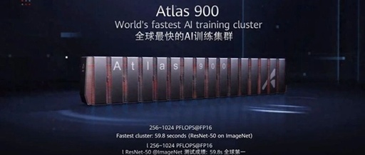
“ The U.S. blockade on chip exports to China has made NVIDIA CEO Jensen Huang anxious, as he is well aware of the current level of domestic computing power in China. Recently, Huawei launched the AI computing cluster solution CloudMatrix 384, which may seem similar to others at first glance, but a closer analysis reveals … Read more

From Beginner to Expert in Chip Manufacturing: A Practical Guide to the Complete Semiconductor Processing Flow (Series Four – Complete Wafer Manufacturing Process)

From Beginner to Expert in Chip Manufacturing: A Practical Guide to the Complete Semiconductor Processing Flow (Series Four - Complete Wafer Manufacturing Process)

Overview This chapter will introduce the four basic processes used in wafer manufacturing to form electrical components of integrated circuits on the surface and within the wafer. The circuit design process traces from functional diagrams to the production of photomasks and mask plates. The characteristics and terminology of wafers and chips are described in detail. … Read more

Huawei CM384’s Comeback: How Domestic Computing Power Breaks the Chip Blockade

Huawei CM384's Comeback: How Domestic Computing Power Breaks the Chip Blockade

Click the “blue text” above to follow us The ongoing escalation of the U.S. chip export ban against China is intended to curb the development of artificial intelligence in China, but it unexpectedly highlights Huawei’s technological breakthrough. While NVIDIA CEO Jensen Huang is anxious about China’s progress in computing power, Huawei’s AI computing cluster solution, … Read more