Overview
This chapter will introduce the four basic processes used in wafer manufacturing to form electrical components of integrated circuits on the surface and within the wafer. The circuit design process traces from functional diagrams to the production of photomasks and mask plates. The characteristics and terminology of wafers and chips are described in detail. Finally, a flowchart of a simple semiconductor device manufacturing process is presented.
Objectives
Upon completing this chapter, you should be able to:
-
Identify and explain the four basic wafer operations.
-
Identify the components of a wafer.
-
Draw a flowchart of the circuit design process.
-
Explain the definitions and uses of composite diagrams and mask sets.
-
Draw cross-sections showing the doping sequence of basic operations.
-
Draw cross-sections showing the metallization sequence of basic operations.
-
Draw cross-sections showing the passivation sequence of basic operations.
-
Identify the “components” of integrated circuit chips.
Wafer Manufacturing
The four stages of microchip manufacturing are material preparation, crystal growth and wafer preparation, wafer manufacturing, and packaging. The first two stages were discussed in Chapter Three. This chapter will explain the basics of the third stage—wafer manufacturing.
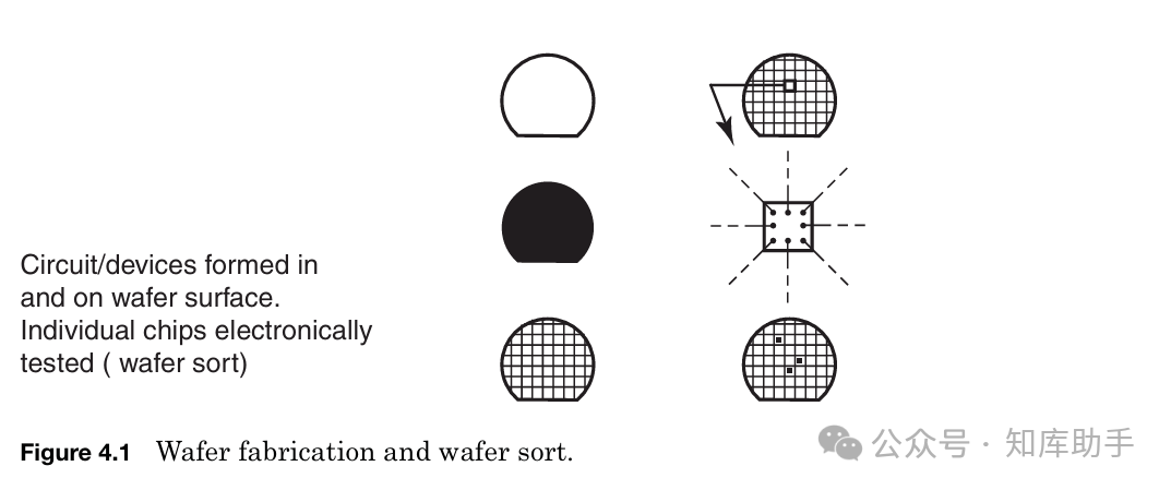
Wafer manufacturing is the process used to create semiconductor devices on the surface and within the wafer. The starting wafer, which is polished, is blank during manufacturing, while at the exit, its surface is covered with hundreds of completed chips (see Figure 4.1).
Wafer Terminology
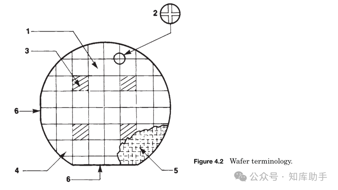
Figure 4.2 shows a completed wafer. The areas on the wafer surface include:
-
Chips, die, devices, circuits, microchips, or strips. All these terms are used to identify the microchip patterns that cover most of the wafer surface.
-
Scoring lines, saw lines, streets, and avenues. These areas are the spaces between chips that allow for the separation of chips from the wafer. Typically, scoring lines are blank, but some companies place alignment targets or electrical test structures within them (see photomask).
-
Engineering die, test die. These chips differ from conventional device or circuit die. They contain special devices and circuit elements for electrical testing during the manufacturing process for process and quality control.
-
Edge die. The edges of the wafer contain partial chip patterns, which are wasted space. Larger chips on the same diameter wafer result in a significant amount of partial chips. Larger diameter wafers reduce the wasted space of larger chips.
-
Crystal planes of the wafer. Cross-sectional views show the crystal structure of the wafer beneath the circuit layers. This diagram shows that the edges of the chips align with the crystal structure of the wafer.
-
Flat surfaces/grooves of the wafer. The wafer has flat surfaces from the preparation stage, which provide information about the crystal orientation and doping polarity of the wafer. The longer flat surface is called the primary flat, while the shorter flat surface is called the secondary flat. The depicted wafer has a primary flat and a secondary flat, indicating that it is a P-type <100> oriented wafer. A 300 mm diameter wafer uses the groove as a crystal orientation indicator. The flat surfaces and grooves also assist in aligning the wafer during many wafer manufacturing processes.
Basic Wafer Manufacturing Operations
There are hundreds of thousands of different types of microchips and their functions. However, they are made using a small number of basic structures (primarily bipolar or MOS structures) and manufacturing processes. This can be compared to the automotive industry. This industry produces a wide variety of products, from cars to bulldozers. However, processes such as metal forming, welding, and painting are common across all factories. Within the factories, these basic processes are applied in different ways to produce the desired products.
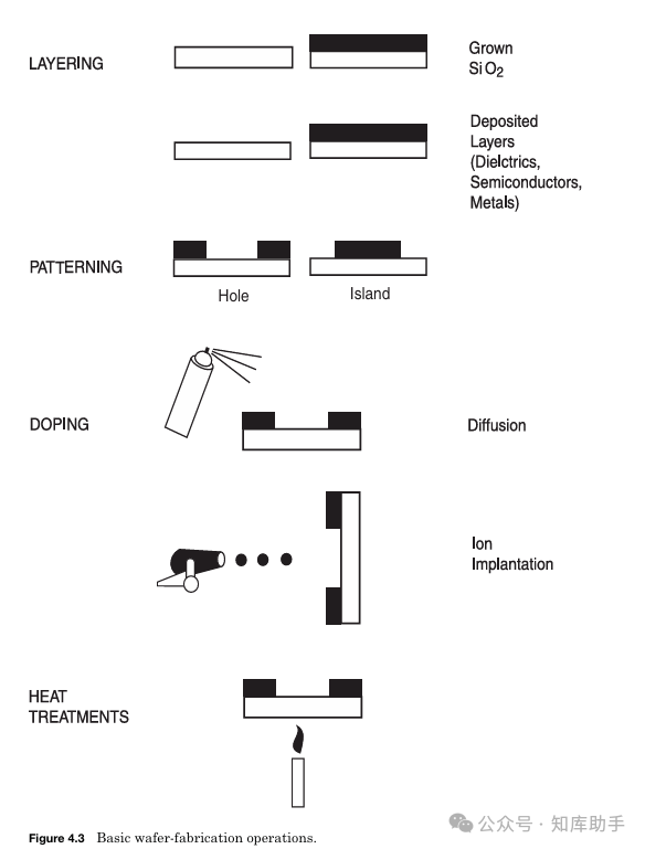
It is the same in microchip manufacturing. Semiconductor companies use four basic operations in an infinite number of sequences and variations to produce specific microchips. These operations include layering, patterning, doping, and thermal treatment (see Figure 4.3).
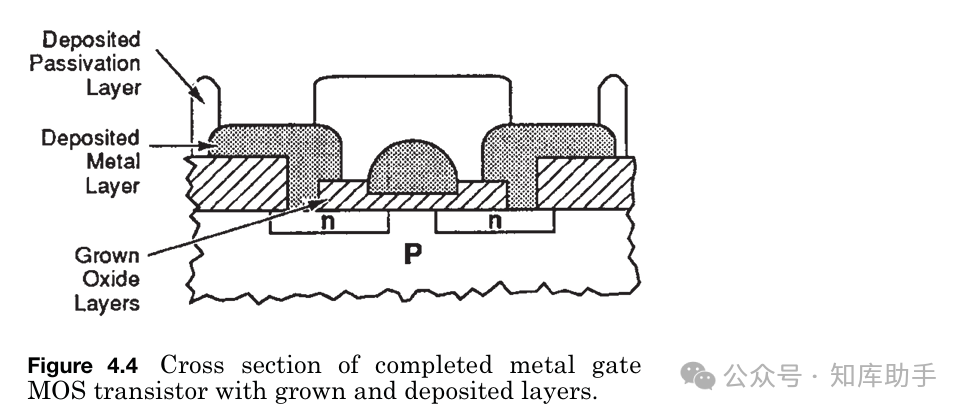
Figure 4.4 shows how these four operations are used to form a doped region on the wafer surface and make contact with a metal conductive layer. A cross-section of a simple metal-oxide-semiconductor (MOS) silicon gate transistor demonstrates how these basic operations are used to create a real semiconductor device.
Layering
Layering is the operation used to add thin layers to the wafer surface. Observing the simple MOS transistor structure in Figure 4.4, multiple layers have been added to the wafer surface. These layers may be insulators, semiconductors, or conductors. They are made from different materials and are grown or deposited through various processes.
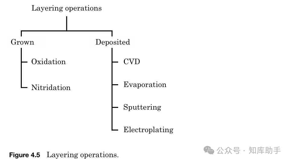
Key technologies include the growth of silicon dioxide layers and the deposition of various materials (see Figure 4.5). Common deposition techniques include physical vapor deposition (PVD), chemical vapor deposition (CVD), evaporation, and sputtering. Electroplating is used to deposit gold metallization on high-density integrated circuits.
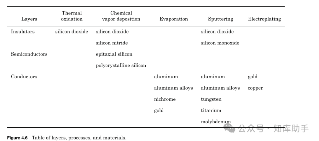
Figure 4.6 lists common layer materials and layering processes. Details of each material are explained in the process chapters. The roles of different layers in the structure are explained in Series Two.
Patterning
Patterning is a series of steps that result in the removal of selected portions of the added surface layer (see Figure 4.7). After removal, the wafer surface is left with a pattern of that layer. The removed material may be a hole in the layer or merely residual islands of material.
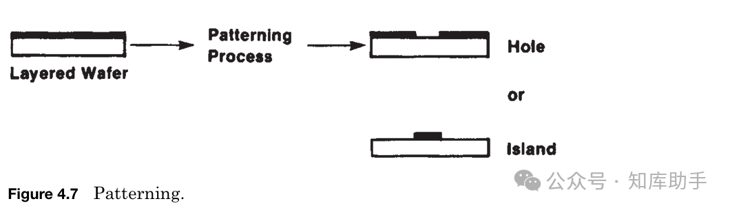
This patterning process is referred to as photomasking, masking, photolithography, and microlithography. During the wafer manufacturing process, various physical parts of transistors, diodes, capacitors, resistors, and metal conduction systems are formed on the wafer surface and above it. These parts are created by sequentially adding materials to the surface and removing portions, combined with the patterning process, to create a layer that leaves specific shapes. The goal of the patterning operation is to create the desired shapes at the precise dimensions (feature sizes) required by the circuit design and to position them correctly on the wafer surface in relation to other components.
Doping Doping is the process of introducing a specific amount of electrically active dopants into the wafer surface through openings in the surface layer.
Figure 4.6 Layer, process, and material table.
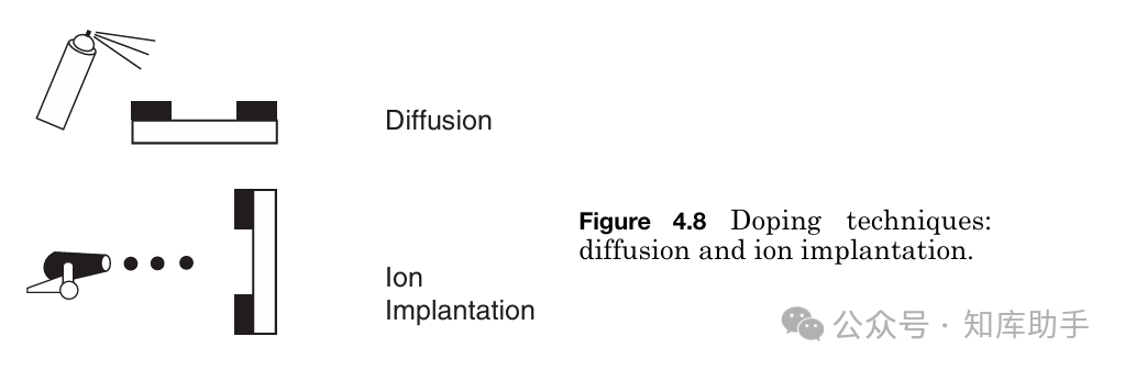
(Figure 4.8) The two techniques are thermal diffusion and ion implantation.
Thermal diffusion is a chemical process that occurs when the wafer is heated to nearly 1000 degrees Celsius and exposed to appropriate dopant vapors. A common example of diffusion is when deodorant vapor diffuses into a room after being released from a pressurized can. The dopant atoms in the vapor enter the exposed wafer surface through this diffusion chemical process, forming a thin film on the wafer surface. In microchip applications, since the wafer material is solid, diffusion is also referred to as solid-state diffusion. Diffusion is a chemical process.
Ion implantation is a physical process. The wafer is loaded at one end of the injector, while the dopant source (usually in gas form) is located at the other end. At the source end, the dopant atoms are ionized (charged) and accelerated to high speeds, sweeping across the wafer surface. The momentum of the atoms drives them into the wafer surface, much like a projectile from a cannon embedding into a wall.
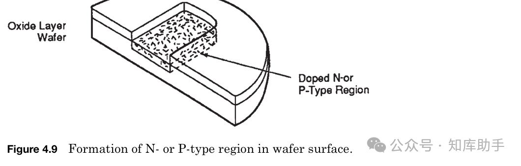
The goal of the doping operation is to create pockets rich in electrons (N-type) or rich in electrical holes (P-type) on the wafer surface (Figure 4.9). These pockets form the electrically active regions and N-P junctions required for the operation of transistors, diodes, capacitors, and resistors in the circuit.
Thermal Treatment
Thermal treatment is the operation of simply heating and cooling the wafer to achieve specific results (Figure 4.10). During thermal treatment,
Figure 4.10 Main thermal treatment table.
| Operation | Heat treatment |
|---|---|
| Patterning | Soft bake Hard bake Post exposure bake(develop) |
| Doping | Post ion implant anneal |
| Layering | Post metal deposition and patterning anneal |
No additional materials are added or removed from the wafer during processing operations, although contaminants and vapors may evaporate from the wafer surface. An important thermal treatment occurs after ion implantation. The injection of dopant atoms disrupts the crystal structure of the wafer, which is then repaired through thermal treatment at approximately 1000°C (called annealing). Another thermal treatment occurs after the formation of metal conductive strips on the wafer. These strips are responsible for the current between various devices in the circuit. To ensure good conductivity, the metal is “alloyed” to the wafer surface through thermal treatment at 450°C. The third important thermal treatment is heating the wafer with a photoresist layer to drive off solvents that interfere with precise patterning.
Circuit Design
Circuit design is the first step in creating microchips.
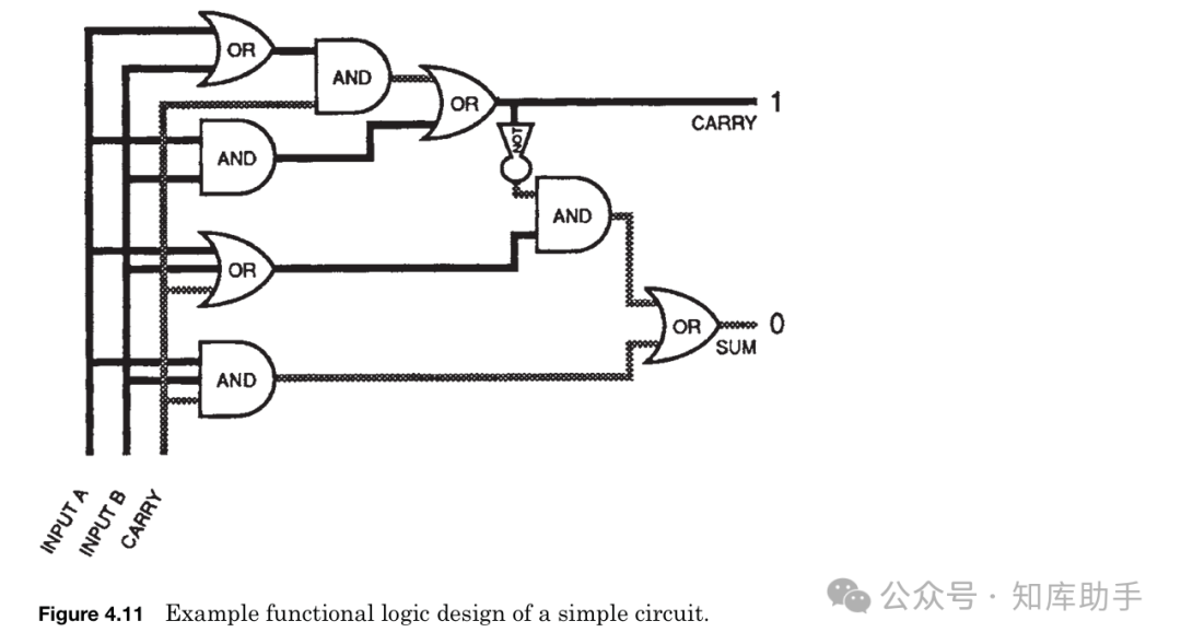
Circuit designers start with a functional block diagram of the circuit, such as the logic diagram in Figure 4.11. This diagram lists the main functions and operations required by the circuit.
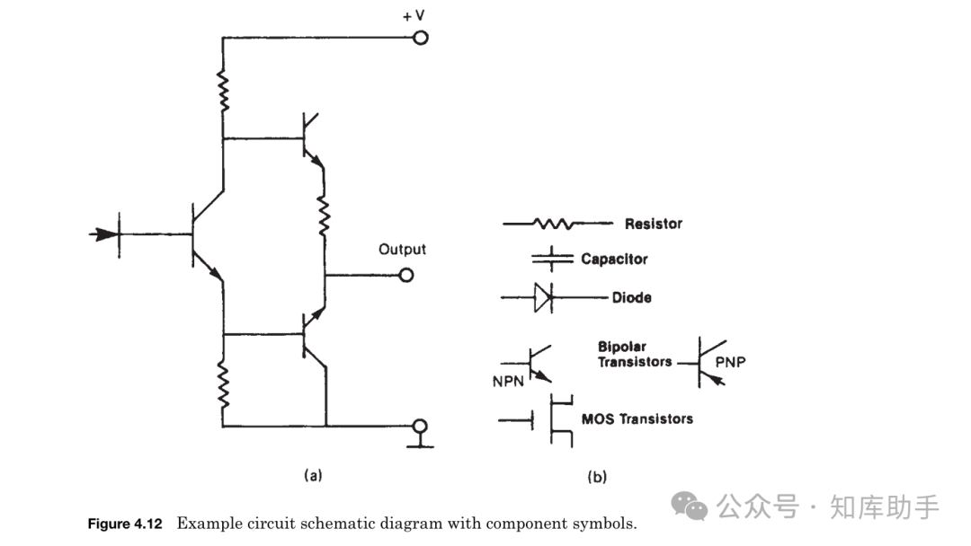
Next, the designer converts the functional diagram into a schematic (Figure 4.12). This diagram identifies the number and connections of various circuits. Each component is represented by a symbol. The circuit schematic also includes the electrical parameters (voltage, current, resistance, etc.) required for the circuit to function.
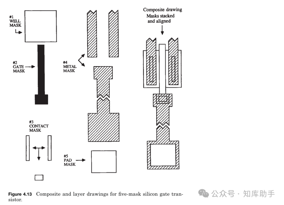
The third step, circuit layout, is unique to semiconductor circuits. The operation of the circuit depends on several factors, including material resistivity, physical properties of the materials, and the physical sizes of the individual components. The placement of components relative to each other is another factor. All these considerations determine the physical layout and size of the components/devices/circuits. The layout begins with using complex computer-aided design (CAD) systems to convert each circuit component into its physical shape and size. Through the CAD system, the circuit is constructed, accurately replicating the final design. The result is a composite image showing the patterns of all sublayers on the circuit surface. This drawing is called a composite diagram (see Figure 4.13). The composite diagram is similar to a blueprint of an office building showing all floors from above.However, the dimensions of the composite materials are much larger than the final circuit dimensions. Both buildings and semiconductor circuits are constructed layer by layer. Therefore, the composite drawings need to be divided into the layouts of each individual layer in the circuit. Figure 4.13 shows the composite materials and individual layer patterns of a simple silicon gate metal-oxide-semiconductor transistor. Each layer drawing is digitized (digitization is the process of converting layer drawings into a digital database) and plotted on a computerized X-Y plotting table.
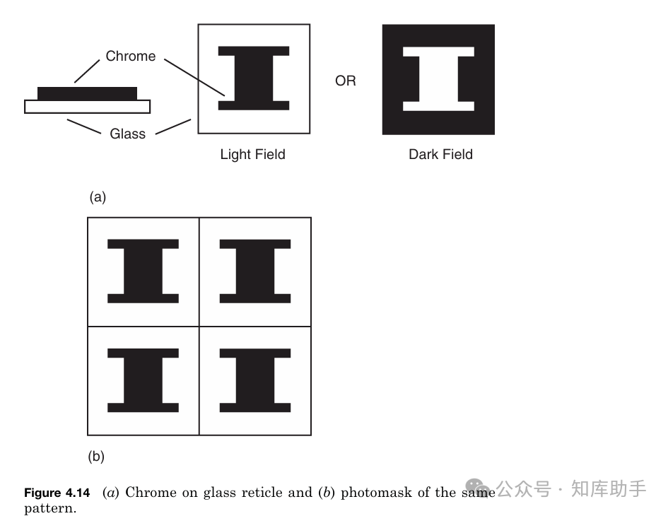
Photomasks and Mask Plates
The patterning process is used to create the desired layer patterns and dimensions on the wafer surface and within it. Transferring the digitized patterns to the wafer surface requires several steps. For the photolithography process, there is an intermediate step called the photomask. The photomask is a “hard copy” of a single drawing recreated on a thin layer of chrome deposited on a glass or quartz plate (see Figure 4.14a). The photomask can be used directly in the patterning process or to create a photomask. The photomask is also a glass plate coated with a thin layer of chrome. After production, it is covered with many copies of circuit patterns (see Figure 4.14b). It is used to pattern the entire wafer surface in a single pattern transfer.
Photomasks and masks are produced in a separate department or purchased from external suppliers. They provide a set of independent photomasks or a set of masks (mask set) for each type of circuit for the manufacturing area.
Example Manufacturing Process
The manufacturing of circuits begins with a polished wafer. The cross-sectional sequence in Figure 4.15 shows the basic operations required to form a simple MOS silicon gate transistor structure. Below is an explanation of each operation in the manufacturing process.
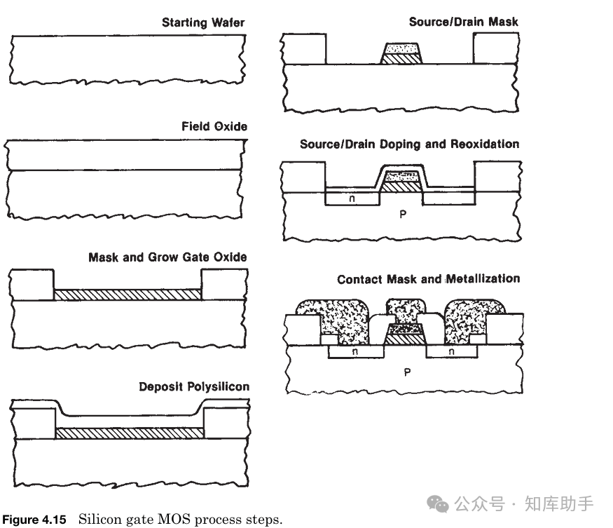 Step 1: Layering operation. The process begins with oxidizing the wafer surface to form a thin protective layer that acts as a doping barrier. This layer of silicon dioxide is called field oxide.
Step 2: Patterning operation. The patterning process leaves a hole in the field oxide, defining the locations of the source, gate, and drain regions of the transistor.
Step 3: Layering operation. Next, the wafer undergoes a silicon dioxide oxidation operation. A thin film of oxide is grown on the exposed silicon. It will become the gate oxide.
Step 4: Layering operation. In step 4, another layering operation is used to deposit a layer of polysilicon. This layer will also become part of the gate structure.
Step 5: Patterning operation. Openings are etched in the oxide/polysilicon layer to define the source and drain regions of the transistor.
Step 6: Doping operation. A doping operation is used to create an N-type pocket in the source and drain regions.
Step 7: Layering operation. Another oxidation/layering process grows a layer of silicon dioxide over the source/drain regions.
Step 8: Patterning operation. Holes are etched in the source, gate, and drain regions, called contact holes.
Step 9: Layering operation. A thin conductive metal layer, usually aluminum alloy, is deposited over the entire wafer.
Step 10: Patterning operation. After deposition, the wafer returns to the patterning area, where portions of the metallization layer are removed from the chip area and scribe lines. The remaining portions connect all surface components according to the precise pattern required by the circuit design.
Step 11: Thermal treatment operation. After the metal patterning step, the wafer undergoes a heating process in a nitrogen atmosphere. The purpose of this step is to cause the metal to “alloy” with the exposed source and drain regions and the gate region to ensure good electrical contact.
Step 12: Layering operation. The final layer of the device is a protective layer, commonly known as a scratch layer or passivation layer. Its purpose is to protect the components on the chip surface during testing and packaging, as well as during actual use.
Step 13: Patterning operation. The last step in the sequence is a patterning process that removes portions of the scratch protective layer covering the metallization pads on the chip perimeter. This step is called the pad mask.
These 13 steps demonstrate how to construct a specific transistor structure using the four basic manufacturing operations. Other necessary circuit components (diodes, resistors, and capacitors) are also formed in other areas of the circuit during the transistor formation process. For example, in this sequence, the resistor pattern is placed on the wafer simultaneously with the source/drain pattern of the transistor. Subsequent doping operations create the source/drain and resistor. Other types of transistors, such as bipolar and silicon gate metal-oxide-semiconductor (MOS), are also formed through these four basic operations using different materials and different sequences.
Typically, circuit components are formed in the first batch of manufacturing operations, known as the front-end-of-line (FEOL) processes. In subsequent operations, various metallization layers that connect the circuit components are added to the wafer surface. These operations are referred to as back-end-of-line (BEOL) processes.
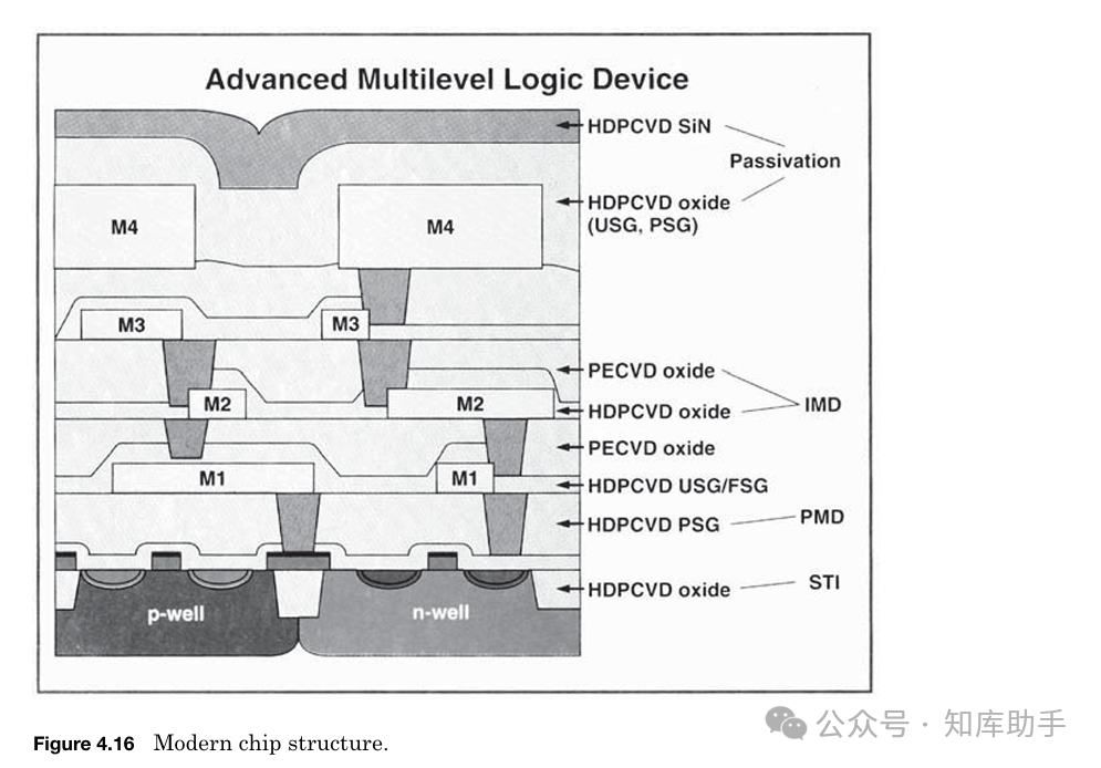
Modern chip structures are much more complex than the processes just described. They have multiple layers and dopant pockets, including multiple layers added to the surface, as well as alternating conductor layers with dielectric materials (see Figure 4.16).
Achieving these complex structures requires many processes. Each process, in turn, requires multiple steps and sub-steps. A speculative process for a 64-GB CMOS device may require 180 major steps, 52 cleaning/stripping operations, and up to 28 masks. However, all major steps are one of the four basic operations.
Figure 4.17 lists the basic operations and their corresponding principle process options. By the time the industry manufactures circuits with gate widths of a few atoms and stacked metal layers above the circuit, the number of process steps will be 500 or more.
Figure 4.17 Summary of wafer factory operations/processes.
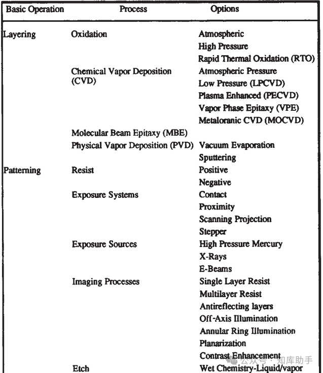
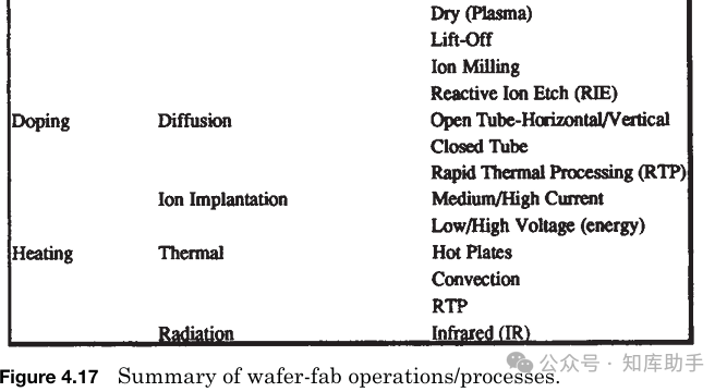
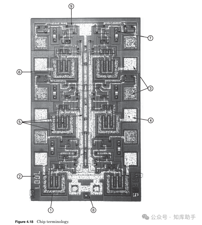
Figure 4.18 shows an optical microscope photo of an MSI/bipolar integrated circuit. This integration level was chosen to see some surface details. The components of higher density circuits are so small that they cannot be distinguished in an optical microscope photo of the entire chip. Features of the chip include:
-
A bipolar transistor
-
The designated number of the circuit
-
Pads for connecting the chip to the package
-
A contamination on the pad
-
Metal lines
-
Scribe (separation) lines
-
Unconnected components
-
Mask alignment marks
-
Resistors
Wafer Sorting
Following the wafer manufacturing process is a very important testing step: wafer sorting. This test is the report card of the manufacturing process. During testing, each chip undergoes electrical performance and circuit functionality tests. Wafer sorting is also known as chip sorting or electrical sorting.
During testing, the wafer is held in a vacuum fixture and aligned with thin electrical probes that contact each pad on the chip (see Figure 4.19). The probes are connected to a power source that records the results of the tests. The number, order, and type of tests are guided by a computer program. Wafer probers are automated, so once the probes are aligned to the first chip (manually or through an automatic vision system), subsequent tests can be performed without operator assistance.
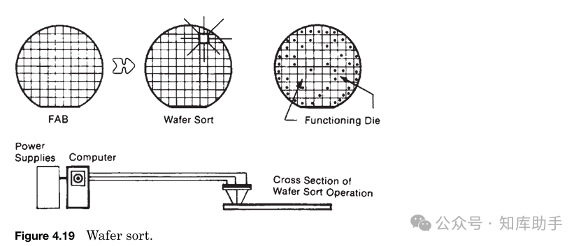
The goals of the testing are threefold. First, to identify working chips before entering the packaging operation. Second, to characterize the electrical parameters of the devices/circuits. Engineers need to track parameter distributions to maintain process quality levels. The third goal is to record the locations of working and non-working chips to provide overall performance feedback to the factory personnel. The locations of working and non-working chips are recorded on a wafer map in the computer. Older technologies would drop a dot of ink on non-working chips.
Wafer sorting is one of the major yield calculations in the chip production process. As chips become larger and denser, their costs become more expensive. These chips require more time for probing, and the power, wafer handling machinery, and computer systems must also be more complex to perform tests and track results. Visual systemsAs chip sizes increase, the manufacturing process must also continuously advance in complexity and cost. Reducing chip testing time is also a challenge. Chip designers are required to incorporate test modes for memory arrays. Once the characteristics of the chip are fully determined, test designers are exploring ways to simplify the test sequence using simplified tests, performing scan tests of the circuits, and parallel testing different parts of the circuit.
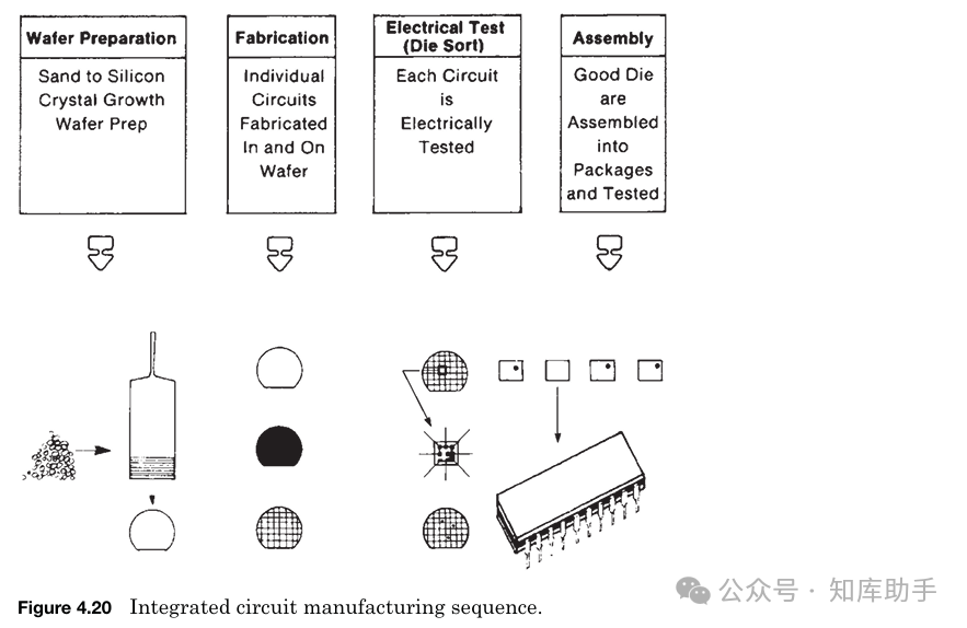
Packaging
Most wafers proceed to the fourth stage, known as packaging (see Figure 4.20). The wafers are transferred to the packaging area at the same location or a remote site. Many semiconductor manufacturers package chips in offshore facilities. At this stage, the wafers are divided into individual chips, and working chips are incorporated into protective packaging. Some chips are incorporated directly into electrical systems without packaging.
The semiconductor microchip manufacturing process is long, complex, and varies based on product type, integration level, feature size, and other factors. By dividing it into four stages, it becomes easier to understand specific processes. By identifying the four basic operations performed on the wafer, a further understanding of wafer manufacturing can be achieved. Several simple processes have been used to illustrate the basic wafer manufacturing operations.
Review Questions
-
List one layering technique.
-
Which basic operation uses ion implantation technology?
-
List the four basic wafer manufacturing operations.
-
Draw and label a cross-section for an oxidation/patterning/doping sequence.
-
Describe a composite diagram.
-
Which basic operation uses a photomask?
-
What parameter is tested during wafer sorting (wafer thickness, defect density, circuit functionality)?
-
Which step in the circuit design process uses computer-aided design systems?
-
What is the purpose of chip packaging? What is the role of the holes created in the contact mask step?
References
-
R. Kopp, “Kopp Semiconductor Engineering,” September 1996.
-
R. Iscoff, “VLSI Testing: The Stakes Are Higher,” Semiconductor International, September 1993, p. 58.