Application-Specific Integrated Circuits (ASICs) are essential in modern circuit design. They are a diverse class of integrated circuits that help designers optimize complex electronic devices.
In the past, discrete components—mainly resistors, capacitors, inductors, transistors, and diodes—were sufficient for many electrical design projects. Nowadays, it is rare to find a circuit board without at least one integrated circuit, while boards filled with various shapes and sizes of integrated circuits are quite common. The popularity of integrated circuits in modern circuit design is largely due to engineers’ ability to easily find, evaluate, purchase, and use a wide variety of microchips. However, off-the-shelf integrated circuits sometimes cannot directly provide the most optimized solutions, which is when engineers might consider using application-specific integrated circuits.
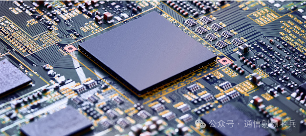
1. What is an Application-Specific Integrated Circuit (ASIC)?
There is no official definition for ASIC, and many electronics professionals have different views on what exactly constitutes an ASIC or whether a certain component qualifies as one. I once saw a definition in a magazine that serves as a good reference:
“An application-specific integrated circuit is an integrated circuit designed for a specific customer, application, or market, using a cell-based design methodology, selecting necessary functional modules from a cell library, connecting them, and simulating to achieve the required system functionality and performance level. This definition does not include integrated circuits designed using traditional ‘custom’ design methods.”
The first part of this definition—integrated circuits designed for a specific customer, application, or market—is a broader and more common understanding of the term. However, the second part is quite useful as it distinguishes “ASIC” from merely “custom integrated circuits.” If ASIC were the same as custom integrated circuits, why would we need a specific term for ASIC?
The complete definition indicates that ASICs can provide custom functionality without going through the entire custom design process. Instead, their custom functionality is achieved through a process similar to designing printed circuit boards. When drawing schematics, we select components from a library, connect them, and sometimes verify parts of the schematic through simulation. When designing an ASIC, designers select functional modules from the library, connect them, and verify functionality and performance through simulation.
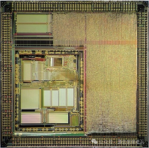
For example, the following diagram shows an ASIC that combines a standard Digital Signal Processor (DSP) core with additional circuits required for the specific application desired by the customer.
2. What does “Application-Specific” mean in ASIC?
The term “application-specific” in ASIC can be somewhat misleading. In current circuit design terminology, “application” generally refers to the actual use of the electronic device. In simple terms, it means what specific task the device is designed to perform.
However, in reality, application-specific integrated circuits often do not target just one specific use, nor are they limited to a single application. For example, a highly integrated data converter ASIC may primarily be designed for medical imaging but can also be effectively used in industrial video processing or automotive multi-channel sensor networks. Another common example is a system-on-chip ASIC that was initially designed for smartphones but can be utilized in many other applications due to its integrated functionalities.
Therefore, I believe terms like “Task-Specific Integrated Circuit (TSIC)” or “Function-Specific Integrated Circuit (FSIC)” might be more accurate. However, these terms do not roll off the tongue as easily as ASIC. Overall, the design purpose of an ASIC is to enable a chip to efficiently perform a series of specific tasks. Even if these tasks were initially designed for a specific application, the ASIC may be more useful and suitable in many other scenarios than off-the-shelf integrated circuits.
3. Classification of ASICs
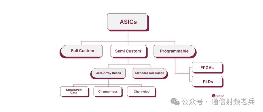
1. Fully Custom ASIC
This type of ASIC is entirely designed from scratch for a specific application. Every aspect of the chip, from logic gates to circuit layout, is customized to meet the precise requirements of the target application. Fully custom ASICs offer the highest performance and lowest power consumption but come with the highest design and manufacturing costs and the longest development time. Generally, this type of ASIC is only used when production volumes are sufficiently large or when performance requirements are particularly stringent, justifying the additional costs and effort.
2. Semi-Custom ASIC
Semi-custom ASICs include standard cell ASICs and gate array ASICs, striking a balance between customization and cost.
– Standard Cell ASIC: In standard cell-based ASIC design, there is a library of pre-designed logic cells, such as AND gates, OR gates, multiplexers, and flip-flops. These cells are standardized and specifically intended for ASIC chip design. ASIC chips typically contain a standard cell area or flexible module composed of these arranged cells and may also integrate macro cells like microcontrollers or microprocessors, which are also referred to as macro functions, system-level macros, or fixed modules/function standard modules. The mask layers of standard cell ASICs can be customized, allowing designers to strategically place standard cells on the chip to efficiently utilize space and optimize performance. This design method is also known as C-BIC.
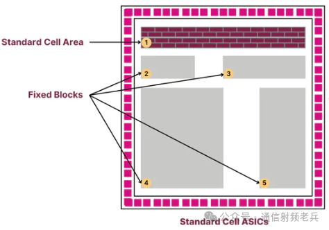
– Gate Array ASIC: Gate array ASICs are a type of semi-custom ASIC where pre-made transistors are present on the silicon wafer. Designers cannot change the positions of the transistors but can alter their interconnections through the initial metal layers of the chip. The design will use a gate array library to configure, typically forming channel-type, non-channel-type, or structured gate arrays, each with different connection methods. This method is called mask gate array, and circuit design relies on basic array patterns and basic cells.
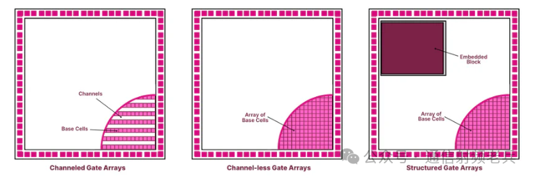
– Channel-Type Gate Array: There are pre-defined wiring channels between logic cells for connecting lines, suitable for standardized designs that require flexible interconnection paths.
– Non-Channel-Type Gate Array: There are no pre-defined wiring channels, allowing interconnect lines to be placed directly above the cells, resulting in a more compact design and higher chip density.
– Structured Gate Array: Combines pre-defined logic blocks with customizable interconnect layers, balancing design flexibility and rapid development.
3. Programmable ASIC
– PLD: This is a type of digital integrated circuit that can implement various logic operations through programming. It is often used in many applications to realize custom logic circuits without the need for dedicated semiconductor custom manufacturing.
– FPGA: Can be reprogrammed and used for various applications. After manufacturing, users can configure it according to different requirements.
4. ASIC Design Process
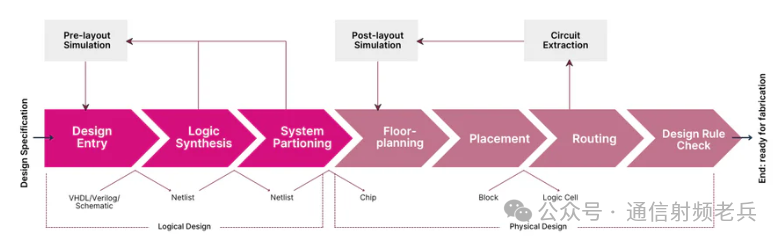
– Design Input: This phase involves developing the microarchitecture using hardware description languages such as VHDL, Verilog, and System Verilog.
– Logic Synthesis: This step generates a netlist that lists the logic cells, their interconnections, and other necessary components based on the hardware description language code.
– System Partitioning: Here, the large chip is divided into manageable ASIC-sized parts, making design and processing more efficient.
– Pre-Layout Simulation: This phase conducts a simulation to identify and correct errors in the design.
– Layout Planning: This step determines the arrangement of netlist modules on the chip.
– Placement: This step determines the specific locations of cells within each module.
– Routing: This phase establishes physical connections between modules and cells.
– Extraction: This step primarily assesses the electrical characteristics of the connections, such as resistance and capacitance.
– Post-Layout Simulation: This is the final simulation that tests the functionality of the entire system, including the effects of interconnect loads, before the design is sent for manufacturing.
5. ASIC Design Cycle
Even with the help of functional modules from the cell library, designing and verifying a custom integrated circuit is not a simple task. If designers cannot find the required functionality or performance in off-the-shelf integrated circuits, the first approach is usually to “look again.” If they still cannot find it, programmable logic devices—such as FPGAs or CPLDs—may be a reliable choice.
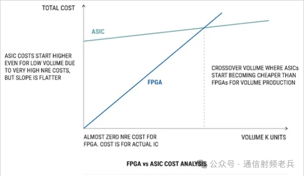
Developing an ASIC can take several months or even years, requiring an investment of tens of millions to hundreds of millions of RMB to produce the first chip. Therefore, typically only projects with high production volumes and stringent performance requirements are deemed worth the time and money to develop ASICs. When production volumes are sufficiently large, ASICs actually have cost advantages. Overall production costs decrease because the savings from components and assembly costs far exceed the ASIC development costs allocated to each chip.
The following chart compares the development costs of ASIC-based solutions with those based on programmable logic. It shows that as production volume increases, ASIC solutions ultimately achieve lower total production costs.
The following lists the main stages of an ASIC design project:
– Define the specifications of the ASIC based on system requirements and other relevant constraints.
– These specifications provide a framework for high-level architectural design.
– The high-level architecture will be transformed into lower-level logic. Like FPGAs and CPLDs, hardware description languages (VHDL and Verilog) have become very useful tools in ASIC design.
– Test the design to verify that functionality and timing meet requirements.
– The logical design must be converted into a physical layout.
– Once the physical layout is validated, the project can proceed to the tape-out and manufacturing stages.
– After manufacturing and packaging, the ASIC undergoes electrical testing and is then integrated into prototypes for laboratory and field testing.
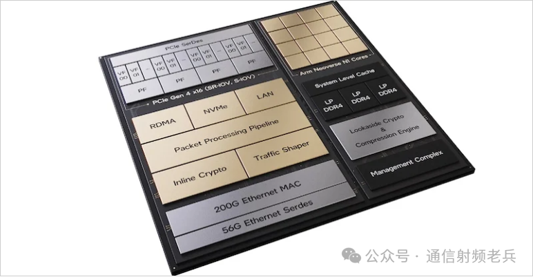
This diagram illustrates the high-level architecture of an ASIC designed for “cloud services and communication service providers” as a “programmable network device.”
6. Advantages of ASICs
– High Performance: ASICs are custom-designed for specific applications, so they generally outperform general-purpose integrated circuits.
– Low Power Consumption: Because ASICs are optimized for specific uses, they typically consume less power for the same tasks compared to other types of integrated circuits.
– Small Size: ASICs can integrate many functions into a small chip, reducing the overall size of the device.
– Low Unit Cost: Although the initial development costs are high, the unit cost can drop significantly during mass production.
– High Security: Custom designs make it difficult for others to reverse-engineer the hardware, enhancing security.
– Fewer Components: Integrating multiple functions reduces the number of discrete components needed, simplifying construction and increasing reliability.
7. Applications of ASICs
The unique characteristics of ASICs have transformed the electronics manufacturing industry, allowing for smaller chip sizes and higher logic gate densities per chip. ASIC chips are typically used in high-end applications, such as serving as IP cores in satellites, being critical in ROM production, and being utilized in microcontrollers, as well as in various medical and research fields. Currently, one of the most notable applications of ASIC technology is in Bitcoin mining.
8. Differences Between ASIC and FPGA
ASICs are semiconductor chips custom-designed for specific tasks and are not suitable for general scenarios. Once manufactured, these circuits cannot be reprogrammed. In contrast, FPGAs have programmable hardware, offering flexibility and can be reconfigured after production. A more detailed comparison is as follows:
| Feature | FPGA | ASIC |
| Flexibility | High (reprogrammable) | Low (not reprogrammable) |
| Performance | Lower than ASIC | Higher for specific tasks |
| Power Consumption | Higher than ASIC | Lower (optimized for efficiency) |
| Development Cost | Low (no non-recurring engineering costs) | High (non-recurring engineering costs) |
| Unit Production Cost | Higher than ASIC | Lower (optimized for efficiency) |
| Time to Market | Shorter (reprogrammable, highly adaptable) | Longer (affected by design and manufacturing processes) |
| Reprogrammability | Yes (algorithms can be changed post-production) | No (design is fixed) |
| Applicable Production Scale | Small to medium scale | Large scale (to offset non-recurring engineering costs) |
| Design Cycle | Shorter | Longer |
In summary, whether to choose FPGA or ASIC depends on specific application requirements. FPGAs excel in adaptability and quick deployment, making them suitable for scenarios that require flexible adjustments, such as rapidly changing environments, prototyping, and small to medium-scale production. On the other hand, ASICs stand out in efficiency, with optimized performance and lower power consumption, making them more suitable for large-scale, stable-demand applications—where the high upfront costs can be offset by the benefits of mass production. Ultimately, the choice between FPGA and ASIC should consider factors such as flexibility requirements, performance needs, power consumption, and production scale.
Finally, to summarize:
Component integration simplifies construction and enhances reliability. ASICs have unique characteristics that make chips smaller and increase logic gate density, commonly used in satellites, ROM, microcontrollers, and medical research, with Bitcoin mining being a popular application. ASICs are custom-designed for specific tasks and cannot be reprogrammed; FPGAs are programmable and highly flexible. The choice between FPGA and ASIC depends on demand, with FPGAs being adaptable and quick to deploy, suitable for changing requirements, prototyping, and small to medium-scale production; ASICs are efficient, high-performing, and low-power, suitable for large-scale stable demands, where the high initial costs can be offset by the benefits of mass production, requiring a comprehensive consideration of various factors.
Check out our previous high-scoring articles; there’s always one that can help you:
RF-related knowledge:
Basic RF Knowledge—All About RF Connectors
Basic RF Knowledge—Review of Smith Charts
Introducing Several Useful and Free Tools for Viewing S-Parameters
Basic RF Knowledge—Understanding Circulators
Basic RF Knowledge—Do You Really Know What a Balun Is?
Basic RF Knowledge—Can’t Tell the Difference Between Baluns, Transformers, Magic T, and Bridges?
Basic RF Knowledge—Power Measurement of Modulated Signals
Basic RF PCB Design Knowledge (Part 1)
Basic RF Knowledge—Review of VSWR, Return Loss, and Mismatch Loss Concepts
Basic RF Knowledge—Understanding Bias Tee
Basic RF Knowledge—What You Should Know About Low Noise Amplifiers (LNA)
Basic RF Knowledge—What You Should Know About RF Couplers/Splitters and Couplers
Basic RF Knowledge—Introduction to Impedance Matching
Basic RF Knowledge—Introduction to Free Online Calculation Tools for RF Metrics (Part 1)
Basic RF Knowledge—What is Load Pull Used For in PAs?
Basic RF Knowledge—Understanding RF Attenuators in One Article
Basic RF Knowledge—Differences Between SAW and BAW Filters
Basic RF Knowledge—Review of S-Parameter Concepts
Basic RF Knowledge—What are Pi and T Attenuators?
Basic RF Knowledge—Understanding What Q Value of Filters Is
Basic RF Knowledge—What is Noise Figure (NF)?
PA-related knowledge:
Introducing Digital Predistortion (DPD) Technology in Simple Terms
Understanding Memory Effects in Power Amplifiers (PA)
Digital Predistortion (DPD) Technology: Unlocking New Secrets to Improve Power Amplifier Efficiency!
Understanding Memory Effects in Power Amplifiers (PA)
Basic RF Knowledge—Introduction to Parameters Related to Power Amplifiers (PA) (Part 1)
Basic RF Knowledge—Discussing Why Doherty Structures Can Improve PA Efficiency
Introducing Several Design Methods for GaN Nitride Power Amplifiers Based on Doherty Structures
Revolutionizing Power Amplifiers in the 5G Era: How GaN Nitride Leads Efficient Communication
What is a Load Pull System, and What is it Used For?
Discussing PA VBW
Discussing Protection Methods for RRU Power Amplifiers (PA)
Analyzing the Role of GaN Nitride Power Amplifiers in 5G
How to Improve the Efficiency of Power Amplifiers Using Envelope Tracking Technology.
How to Optimize 5G PA Performance Through PAPR and CCDF Metrics
Basic RF Knowledge—Discussing Amplifiers from Class A to Class H
Transceiver-related knowledge:
Sharing Knowledge About Transceiver Chips (Part 1)
Sharing Knowledge About Transceiver Chips (Part 2)
Sharing Knowledge About Transceiver Chips (Part 3)
Introduction to Transceiver Basics—Types of Transmitters and Receivers
Basic Knowledge of Transceivers—The Impact of Clock Noise on Receivers
Popularizing DDC and DUC in RRU Digital Baseband Processing
Basic Knowledge of Transceivers—What is Receiver Sensitivity?
Basic Knowledge of Transceivers—Introduction to Automatic Gain Control (AGC) Functionality
ADC/DAC-related knowledge:
Understanding High-Speed ADC Basic Architecture in One Article
Understanding High-Speed DAC Basic Architecture in One Article
Understanding Delta-Sigma ADC Basics in One Article
Understanding SAR ADC Basics in One Article
Understanding What Clock Jitter Is and Its Impact in One Article
Understanding the Impact of Clock Jitter on ADC Performance in One Article
Understanding Concepts of Bandwidth, Aliasing, and Sampling in ADCs in One Article
Understanding Types of Noise in ADCs in One Article
Understanding the Difference Between SNR and NSD in ADC/DAC in One Article
Understanding Concepts of DDC, DUC, Sampling Rate, and Data Rate in ADC/DAC in One Article
DAC Basic Knowledge—Output Response (Part 1)
DAC Basic Knowledge—Output Response (Part 2)
DAC Basic Knowledge—Output Response (Part 3)
ADC Accuracy Part 1: Are Accuracy and Resolution Different?
Time Domain and Frequency Domain Analysis Methods for ADCs
How to Plan Frequency and Sampling Rates for ADCs
Clock Optimization for RF Sampling ADCs
Serial Communication-related knowledge:
Understanding Serial Communication—Basics of LVDS
Understanding Serial Communication—Basics of I²C
Understanding Serial Communication—Basics of SPI
Understanding Serial Communication—Basics of UART
Clock System-related knowledge:
Understanding Clock and Timing Systems in One Article
Analyzing Some Differences Between JESD204B and JESD204C
PLL Phase-Locked Loop Basic Knowledge (Part 1)
PLL Phase-Locked Loop Basic Knowledge (Part 2)
PLL Phase-Locked Loop Basic Knowledge (Part 3)
Using IEEE 1588 for Time Synchronization in 5G Networks
How Time Synchronization is Propagated in 5G Networks.
Understanding JESD204B Clock Schemes in One Article
RF Measurement-related knowledge:
Understanding RF Signal Sources in One Article
Keysight N5182B Signal Source Waveform File Loading Tutorial
Understanding How to Measure Noise Figure (NF) Using the Y-Factor Method in One Article
Base Station-related knowledge:
Discussing What RRU and BBU Are
Challenges in 5G Base Station Design: Size, Weight, Power Consumption, and Heat Dissipation
The Past and Present of Semiconductor Equipment Manufacturer New Kai
Discussing the Impact of PIM in Base Stations
What is a 5G Small Cell?
Understanding What Base Station Antennas Are.
Digital Signal Processing-related knowledge:
Digital Signal Processing—Real and Complex Modulation
Digital Signal Processing—Introduction to QAM Modulation and EVM
Digital Signal Processing—Introduction to OFDM Basics
Introduction to Fast Fourier Transform (FFT) and Window Functions
Digital Signal Processing—Introduction to Digital Modulation Basics
Link Budget-related knowledge:
Understanding 3GPP TS 36.104 Transmit Link Related Metrics in One Article
Several Methods for Testing RX Noise Figure (NF) in RRU Receive Links
Communication-related knowledge:
Sharing Knowledge Related to EVM (Part 1)
Biographies of Communication Figures—Hedy Lamarr: A Woman of Beauty and Intelligence
Biographies of Communication Figures—Philip Smith: From Amateur Radio Operator to Creator of Smith Charts
Biographies of Communication Figures—Claude Shannon: The Father of Information Theory
Discussing Some Changes from 4G to 5G
Antenna-related knowledge:
Introduction to Active Antenna Systems (AAS) for MIMO Scenarios
Discussing the Evolution of Antennas Under 5G NR
Discussing the Role of Antenna Elements in Phased Arrays
“MIMO Technology Leading 5G Communication: The Perfect Fusion of Speed, Capacity, and Efficiency”
Understanding What an Anechoic Chamber Is in One Article.
Case Analysis:
Case Analysis of Failed DPD Calibration in Base Stations
Case Analysis of Failed EVM Metrics Testing in Transmit Links
Case Analysis of Failed DPD Optimization in RRU Under High Temperatures
Signal Integrity-related knowledge:
In-Depth Analysis of Decoupling Capacitors and Their Functions
Mastering EMC Secrets: Creating Excellent Performance RF PCB Designs
Basic Knowledge of Signal Integrity (SI) (Part 1)
Layer Selection in PCB Design
Discussing Common Mode Noise in Differential Transmission
Discussing What Eye Diagrams Are.
Satellite Communication-related knowledge:
Finding You Across Mountains and Seas: Understanding Satellite Communication
Basic Knowledge of Satellite Communication—Calculating Free Space Loss and Antenna Gain
Basic Knowledge of Satellite Communication—Uplink and Downlink Budgeting
Basic Knowledge of Satellite Communication—Modulation and Coding Methods, Spectral Efficiency, and Throughput