The assembly methods for printed circuit boards (PCBs) include surface mount, wire bonding, and physical contact connectors, with different assembly methods having varying requirements for connection pad sizes.
IPC 6012 and IPC 6018 classify the size requirements for connection pads according to product grades, while domestic standards such as GJB 362, GJB 9491, GJB 4896 and others have adopted the requirements of IPC for level two and three products.
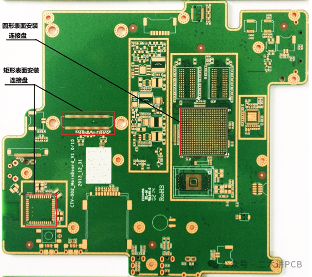
Figure 1: Rectangular and circular mounting pads on the surface of printed circuit boards
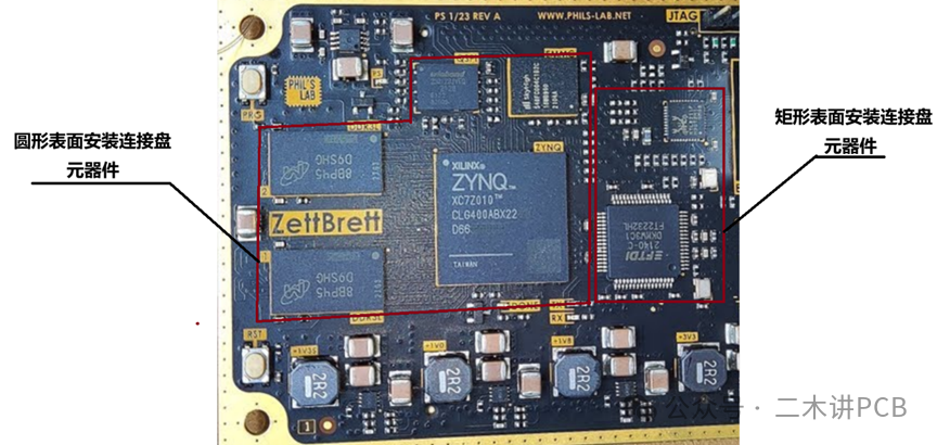
Figure 2: Printed circuit board with a large number of circular and rectangular surface mount connection pad components
(1)Rectangular surface mount connection pads
On the surface of the PCB, most connection pads are rectangular, meeting the installation requirements for rectangular pin chip components (such as chip resistors, chip capacitors, QFP, etc.). The size requirements for rectangular surface mount connection pads are shown in Figure 3.
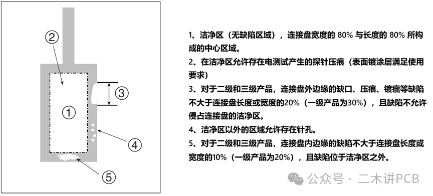
Figure 3: Size requirements for rectangular surface mount pads
(2)Round surface mount connection pads
To meet the demands of multi-pin, high-density, and high-reliability chip packaging, connection pads have been developed in round shapes, such as BGA, CGA, CCGA, etc. The size requirements for round surface mount connection pads are shown in Figure 4.
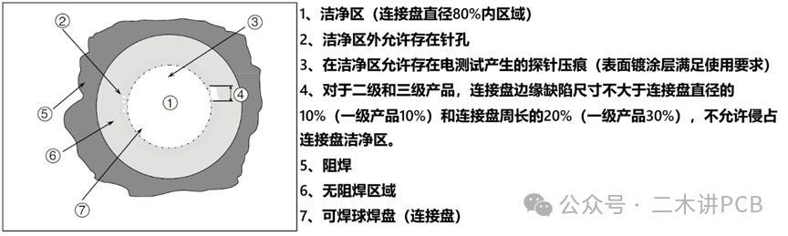
Figure 4: Size requirements for round surface mount connection pads
(3)Wire bonding connection pads
The electrical interconnection between bare chips and substrates (glass, ceramics, or low CTE organic substrates, etc.) is generally achieved through wire bonding. The size requirements for wire bonding connection pads are basically consistent with those of the aforementioned rectangular surface mount connection pads, with the difference being that defects are allowed in the clean area of wire bonding connection pads, and the defect area should not exceed 5% of the clean area. The surface roughness of the clean area should be ≤0.8 micrometers.
(4)Edge connector connection pads
Printed circuit boards with edge connector connection pads can be seen everywhere in daily life, such as U disks, memory sticks, graphics cards, network cards, etc. Domestic standards have clear requirements for the size of defects outside the insertion or contact area of such connection pads: defects such as pits, pinholes, or dents not exceeding 0.15mm are allowed, with no more than 3 defects per connection pad, and the number of defective connection pads should not exceed 30% of the total number of connection pads. The remaining size requirements are consistent with foreign standards, as detailed in Figure 6.
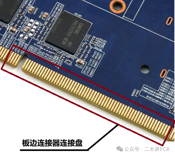
Figure 5: Edge connector connection pads on printed circuit boards
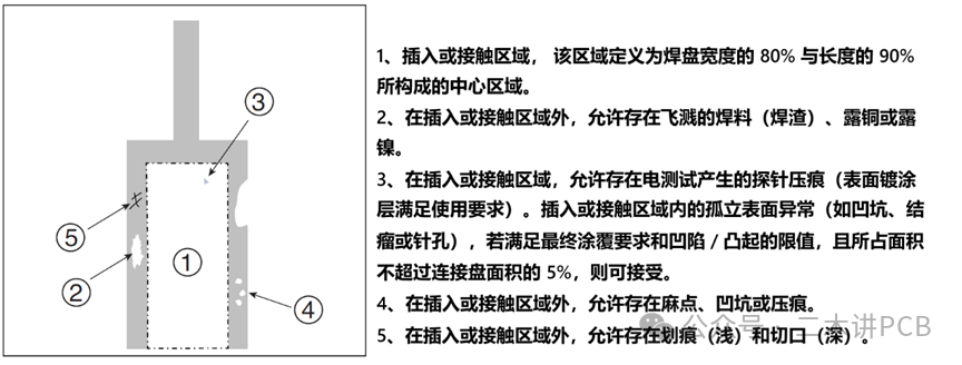
Figure 6: Size requirements for edge connector connection pads