Laminate imperfections in printed circuit boards (Laminate Imperfection) refer to internal and external defects that can be observed from the surface of the printed board. There are more than a dozen types of laminate imperfections, including Measling, Crazing, Delamination/Blistering, Foreign Inclusion, Weave Exposure, Mechanically Induced Disrupted Fiber, Scratch, Dent, Tool Mark, Surface void, Color Variation in Bond Enhancement, and Pink Ring.
Measling:Measling appears as discontinuous white squares or “X” patterns beneath the surface of the substrate, typically associated with thermal stress. Measling is an internal defect in printed circuit boards that does not expand due to thermal stress testing and there is no conclusive evidence that it is a trigger for CAF (Conductive Anodic Filament) growth.
Measling
Crazing:This is an internal condition where fibers within the substrate separate. Micro-cracks can appear at the intersections of fibers or along the length of the fibers. The micro-crack condition manifests as connected white dots or “X” patterns beneath the surface of the substrate, usually related to mechanical stress.
Crazing
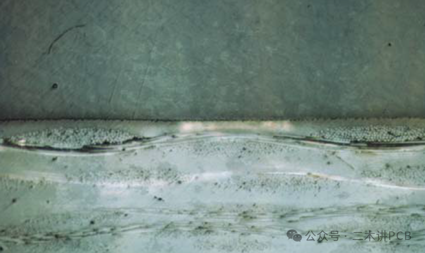
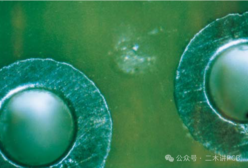
Delamination/Blistering:/Blistering:This refers to local planar separation or bulging between the insulating substrate, copper foil, or solder mask within the printed circuit board.
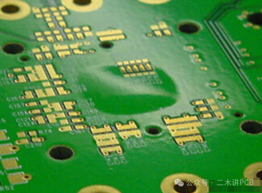
Delamination/Blistering
Foreign Inclusion:This refers to metallic or non-metallic particles that are trapped or embedded within the insulating material. Foreign inclusions can be detected in the raw materials of the substrate, prepreg (B stage), or in the finished printed board.

Foreign Inclusion
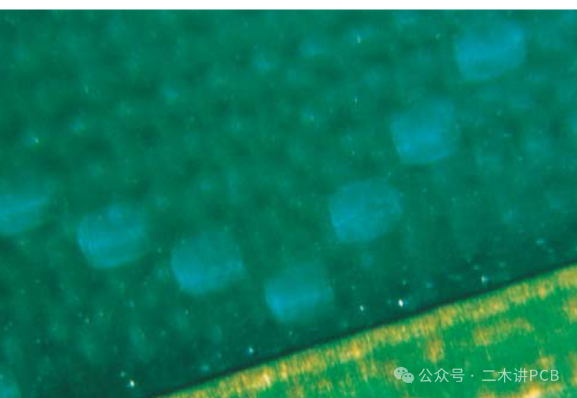
Weave Exposure:This refers to a surface condition of the substrate where unbroken fabric fibers are not completely covered by resin.
Weave Exposure
Mechanically Induced Disrupted Fiber:This refers to fiber breakage caused by mechanical forces during processing.
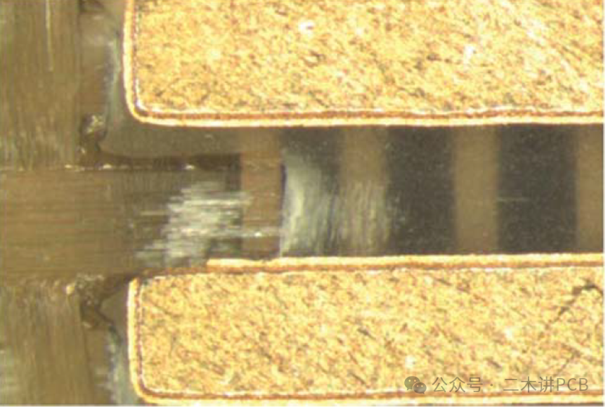
Mechanically Induced Disrupted Fiber
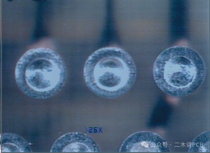
Surface void:This refers to resin defects on the surface of the printed circuit board, resulting in pits.
Surface void
Color Variation in Bond Enhancement:This occurs when the surface of the copper foil undergoes blackening or browning treatment to enhance interlayer bonding strength, forming a layer of cupric oxide and cuprous oxide. Due to contamination from dirty transfer rollers, oxidation/reduction solution pollution, or residual oil on the copper foil surface, the color of the blackened or browned layer may be uneven.
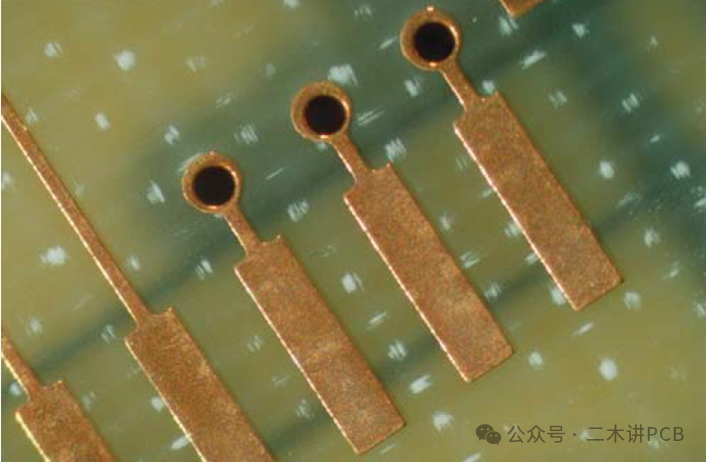
Pink Ring:This occurs when the black or brown bond enhancement layer is corroded by acid or reduction solutions, turning red copper in color. Since it occurs around holes, it is referred to as a pink ring.
Pink Ring
Based on commonly used standards both domestically and internationally, it is recommended that laminate imperfections in printed circuit boards be inspected according to the following criteria:
(1)Measling: Levels 1, 2, and 3 products are allowed to have measling present, while aerospace-grade products are not allowed to have measling. If the size of measling between independent conductors in level 3 products exceeds 50% of the spacing, it indicates a change in materials, equipment, or manufacturing processes, but does not affect product acceptance for use.
(2)Crazing: Cracks must not cause the spacing between conductors to be less than the minimum specified value. For levels 2 and 3 products, micro-cracks must not span more than 50% of the distance between adjacent conductors. Micro-cracks do not expand after thermal stress testing.
(3)Delamination/Blistering: The defect area must not exceed 1% of the single-sided area of the printed circuit board and must not cause the spacing between conductors to be less than the minimum specified value. Delamination/blistering areas do not expand after thermal stress testing. For levels 2 and 3 products, delamination/blistering must not span more than 50% of the distance between adjacent conductors.
(4)Foreign Inclusion: Semi-transparent foreign inclusions are acceptable. For opaque inclusion particles, inclusions must not cause the spacing between conductors to be less than the minimum specified value.
(5)Weave Exposure: Level 3 products must not have weave exposure. For levels 1 and 2 products, weave exposure must not cause the spacing between conductors to be less than the minimum specified value.
(6)Mechanically Induced Disrupted Fiber: Defects must not cause conductor bridging and must not cause the spacing between conductors to be less than the minimum specified value.
(7)Scratch/Dent/Tool Mark: Defects must not cause conductor bridging and must not cause the spacing between conductors to be less than the minimum specified value.
(8)Surface void: The longest dimension must be less than 0.8mm and must not exceed 5% of the single-sided area of the printed circuit board, and surface voids must not bridge conductors.
(9)Color Variation in Bond Enhancement: Randomly occurring color variation areas must not exceed 10% of the total surface area of the conductors.
(10) Pink Ring: Products cannot be rejected due to pink rings; attention should be focused on interlayer bonding strength.