
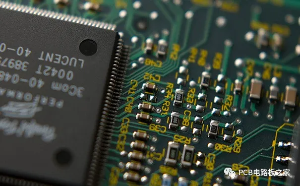
A circuit board, also known as a printed circuit board (PCB) or flexible printed circuit board (FPC), is made from polyimide or polyester film as the substrate, providing high reliability and excellent flexibility. The names of circuit boards include ceramic circuit boards, aluminum oxide ceramic circuit boards, aluminum nitride ceramic circuit boards, PCB boards, aluminum substrates, high-frequency boards, thick copper boards, impedance boards, ultra-thin circuit boards, and printed (copper etching technology) circuit boards. Circuit boards miniaturize and visualize circuits, playing a crucial role in the mass production of fixed circuits and optimizing electrical layouts. So, what are the working layers of a circuit board? What are its components, working principles, and classifications?
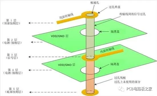
Circuit boards include many types of working layers, such as signal layers, protective layers, silkscreen layers, internal layers, etc. The functions of these various layers are briefly introduced below:
(1) Protective Layer: This layer is primarily used to ensure that areas of the circuit board that do not require tin plating are not plated, thus ensuring the reliability of the circuit board’s operation. The TopPaste and BottomPaste refer to the top solder mask layer and bottom solder mask layer, respectively; TopSolder and BottomSolder refer to the solder paste protective layer and bottom solder paste protective layer, respectively.
(2) Signal Layer: This layer is mainly used for placing components or routing. Protel DXP typically includes 30 intermediate layers, namely MidLayer1 to MidLayer30, which are used for routing signal lines, while the top and bottom layers are used for placing components or copper cladding.
(3) Silkscreen Layer: This layer is primarily used to print component serial numbers, production numbers, company names, etc., on the circuit board.
(4) Internal Layer: This layer is mainly used as a signal routing layer, with a total of 16 internal layers included in Protel DXP.
(5) Other Layers: This mainly includes four types of layers.
DrillGuide (Drilling Position Layer): This layer is mainly used to indicate the positions for drilling holes on the printed circuit board.
Keep-Out Layer: This layer is mainly used to draw the electrical borders of the circuit board.
DrillDrawing (Drilling Drawing Layer): This layer is mainly used to define the shapes of the drill holes.
Multi-Layer: This layer is mainly used to set up multiple surfaces.
Working Principle of Circuit Boards
The working principle of a circuit board is to use insulating materials to isolate the surface copper foil conductive layers, allowing current to flow along pre-designed paths through various components to perform functions such as work, amplification, attenuation, modulation, demodulation, and encoding.
Components of Circuit Boards:
A circuit board mainly consists of pads, vias, mounting holes, traces, components, connectors, and electrical boundaries. The main functions of each component are as follows:
Pads: Metal holes used for soldering component pins.
Vias: There are metal vias and non-metal vias, where metal vias are used to connect component pins between layers.
Mounting Holes: Used to secure the circuit board.
Traces: Electrical networks made of copper film that connect component pins.
Connectors: Components used to connect between circuit boards.
Filling: Copper cladding used for ground networks, which can effectively reduce impedance.
Electrical Boundaries: Used to define the dimensions of the circuit board, ensuring that all components on the circuit board do not exceed this boundary.
Classification of Circuit Boards
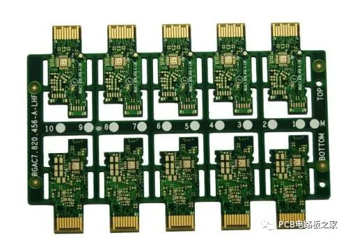
Circuit boards can be classified into three main categories based on the number of layers: single-sided boards, double-sided boards, and multi-layer boards.
Multi-layer Boards: Refers to printed boards that have three or more conductive pattern layers separated by insulating materials, with the conductive patterns interconnected as required. Multi-layer circuit boards are a product of the development of electronic information technology towards high speed, multifunctionality, large capacity, compactness, thinness, and lightness.
Single-sided Boards: On the most basic PCB, components are concentrated on one side, while traces are concentrated on the other side. Since traces only appear on one side, this type of PCB is called a single-sided circuit board. Single-sided boards are usually simple to manufacture and low in cost, but their drawback is that they cannot be used in overly complex products.
Double-sided Boards: An extension of single-sided boards, double-sided boards are used when single-layer routing cannot meet the needs of electronic products. Both sides have copper cladding and traces, and connections between the two layers can be made through vias to form the required network connections.
Circuit boards can also be classified based on their characteristics into flexible boards (FPC), rigid boards (PCB), and rigid-flex boards (FPCB).
Due to the different designs of circuit boards, prices can vary based on the materials used, the number of layers, the size of the circuit board, the quantity produced, the manufacturing process, the minimum line width and spacing, the minimum hole diameter, the number of holes, and special process requirements. Circuit boards have a wide range of applications, including consumer electronics, automotive electronics, communications, medical, military, aerospace, etc., and their market share is continuously increasing.

Screenshots of Some Electronic Books


Screenshots of Some Course PPTs
【Complete Set of Hardware Learning Materials】