As analysts from Yole stated, entering the new decade, “ADAS is helping to climb the autonomous driving ladder defined by SAE in 2014, winning a splendid performance with ‘L2’, ‘L2+’, and now ‘L2++’. But in terms of autonomous driving, reality may not be the same.” Nevertheless, the entire industry is accumulating more experience in achieving the highest level of automation for fully autonomous vehicles (AVs) during this process.
To improve vehicle safety, Advanced Driver Assistance Systems (ADAS) have been in development for over a decade. This technology combines a set of sensors (mainly radar and cameras) with powerful electronic control units, achieving significant breakthroughs over the past decade.
Research from Consumer Reports in the United States shows that 57% of respondents reported having at least one ADAS feature in their cars that prevented them from having an accident. In heavy traffic, drivers often look down at their phones, only to look up and see the car in front has braked. With ADAS, which employs key sensors and components like radar and cameras, such situations can be avoided, ensuring the safety functionality of vehicles.
Academic research has also shown that Automatic Emergency Braking (AEB) can reduce rear-end collisions by 40% and decrease related fatalities by 15%. High technology contributes to the global spread of the ‘Vision Zero’ (no accident driving) concept.
ADAS Functions Becoming Standard in Vehicles
Now, ADAS functions have become standard in many vehicles.The National Safety Council, J.D. Power, AAA, and Consumer Reports have collectively named these ADAS features.There are many terms associated with ADAS; for example, in the 2020 Toyota models, the ADAS features include:FCW (Forward Collision Warning), CABE (City Automatic Emergency Braking)/HABE (Highway Automatic Emergency Braking), PED.AEB (Pedestrian Automatic Emergency Braking), LDW (Lane Departure Warning), LKA (Lane Keeping Assist), BSW (Blind Spot Warning), RCTW (Rear Cross Traffic Warning), etc.
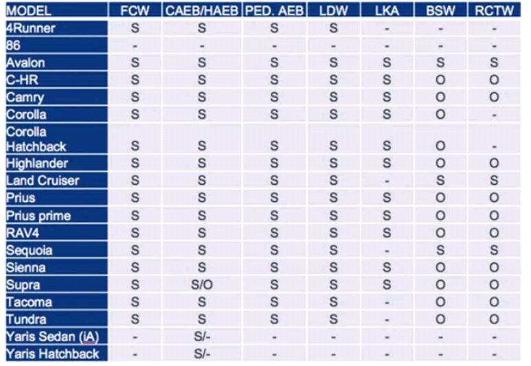
ADAS Features of the 2020 Toyota Models
Some of these features are mandated by regulatory authorities, while others help manufacturers improve vehicle safety ratings; different regions have varying mandatory requirements for ADAS features.
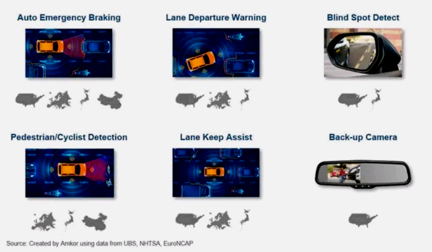
Mandatory ADAS Requirements by Different Regulatory Authorities
Increasing Semiconductor Demands for ADAS
Around the models crossing over 2025-2026, leading OEMs are adopting next-generation architectures. This means clarifying the appearance, internal structure, intelligence, and intersection with future development directions of these models.
David Fritz, Senior Director of Autonomous Driving and ADAS at Siemens Digital Industries Software, said: “OEMs have realized that focusing on modeling the entire system makes more sense, as it allows understanding of how all parts come together to truly address this large and complex issue. It pushes the automotive industry into the realm of semiconductor manufacturing like smartphones and digital TVs, where the application is understood first before building — rather than building first and hoping they will all fit together.”
As vehicles become more feature-rich, the chips supporting these systems are also becoming increasingly complex. For example, ADAS is no longer a standalone domain controller; many previously separate functions have been integrated. Ron Digiusepe, Manager of Automotive IP at Synopsys, said: “As the industry continues to integrate from distributed architectures into multi-SoC complex functionalities, controllers must perform multiple ADAS functions on a centralized module, requiring multi-core processors. It must also support ADAS vision applications like AEB or LKA. AEB will utilize various types of sensors and algorithms, such as AI and vision-based algorithms. This requires more complex processing, so these ADAS domain controllers will use 16nm or 14nm FinFET process chips, and are advancing toward 7nm or even 5nm FinFET processes to accommodate multiple applications with multi-processor cores, such as 8 to 12 Arm 64-bit high-end cores, along with AI/vision accelerators and DSP accelerators.”
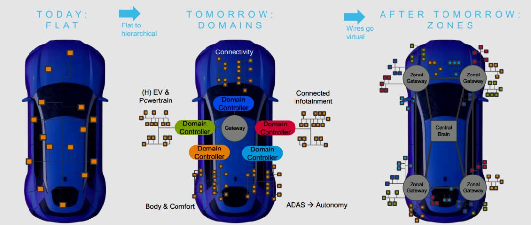
Classic Five-Domain Architecture from ADAS to Autonomous Vehicles
Arm recently published a report highlighting the shift towards heterogeneous computing. Systems like in-vehicle ADAS are becoming increasingly complex and interrelated. Arm states that the diversity of demands requires both a holistic electronic design approach and a more heterogeneous computing architecture.
Prioritizing ADAS Development is Imperative
Undoubtedly, the development of autonomous vehicles will continue, but the deployment of ADAS will be the focus of 2021.
After introducing ADAS features, vehicles have indeed reduced accidents and saved lives. Today, the road for ADAS is still far from complete. ADAS employs sensors like millimeter-wave radar, LiDAR, and monocular/binocular cameras for data decision control; the limitations of algorithms determine that user experience still lags behind human driving, and many ADAS features can only be used in specific scenarios.
Take lane keeping and adaptive cruise control, for example; due to the system’s deliberate control of the vehicle’s position in the lane and the distance from the vehicle ahead, the control of direction and speed can be very stiff. Moreover, ADAS cannot ensure perception of all scenarios, nor guarantee 100% accurate warnings, and does not take proactive measures in any hazardous situations, nor assumes any accident liability. Therefore, under current circumstances, using ADAS should not be taken lightly; drivers must always be responsible for their driving behavior.
Regarding user experience, most ADAS in vehicles have not reached a level that consumers love to use. For users, ADAS can also be overly complex, with so many technical terms that they become bewildered. Therefore, it is urgent for semiconductor manufacturers, Tier 1 suppliers, and OEMs to seriously educate users about the sub-functions of ADAS, especially to help them understand and experience it; otherwise, the promotion and popularization of ADAS will be difficult to achieve. Because the OEMs, who have always touted customer-centricity, also understand that they should provide the features that customers want and are willing to pay for.
Artificial intelligence is empowering ADAS, including self-diagnosing and self-repairing vehicles, which will greatly reduce the incidence of failures. In learning driving modes, new drivers are surrounded by cameras, radars, and LiDAR, effectively avoiding accidents. These systems will ensure that drivers and passengers are safe, informed, entertained, and efficient in their travels. Voice and gesture user interfaces will intuitively understand commands; augmented reality will assist in navigation, providing points of interest or safety alerts, using virtual reality (VR) projections to discover blind spots behind pillars. As all these AI technologies are still in their infancy, hardware systems will need to adjust with the improvements of the systems and extend the lifespan of the systems through OTA updates.
Now, ADAS technology has entered many vehicle models, even though some do not call it ADAS. The next step is how to fuse its functionalities through sensors. Today’s cameras are getting better, and 3D cameras are being deployed, which are only half a step away from LiDAR, and cost about 1/100 of the latter. Of course, in recent years, the cost of LiDAR has also significantly decreased, with startups playing a major role in this field.
ADAS and Its Semiconductor Processes
First, look at the forward safety camera; depending on the required functionality, there are various types of cameras categorized by the number of lenses into monocular, binocular, and trino. They are further classified by distance into long, medium, and short-range cameras. Trino or multi-lens cameras provide stereoscopic vision, estimating distance based on multiple independent images of the same environment obtained from adjacent different perspectives, i.e., triangulation of visual information. Algorithms are then used to process a dense 3D digital representation of the real environment.
In short-range LiDAR, such as Continental’s multifunctional camera MFL4x0, the infrared short-range LiDAR (Light Detection and Ranging) sensor is integrated with a CMOS camera in a compact unit, allowing installation even in small vehicles. Its main function is to classify objects in front of the vehicle with very high reliability and detect imminent collisions; it also has driver assistance features (such as lane departure warning, traffic sign recognition, and intelligent headlight control).
Multifunctional Camera with LiDAR
The ZF TriCam trino camera is a module that integrates “three eyes”, providing crucial information from different perspectives at different distances from the front and sides of the vehicle, ensuring various driving situations are accounted for.
Cameras are essential for object detection. They utilize AI to detect objects like pedestrians or trash bins on the roadside, providing necessary information for the vehicle. Additionally, the greatest advantage of cameras is their ability to measure angles accurately. This allows vehicles to recognize early whether approaching vehicles will turn. If urban traffic requires a wide-angle view to record pedestrians and traffic conditions, then highways require a long-distance and narrow view of 300 meters.
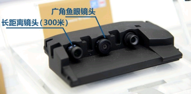
“Three-Eye” Camera Module
The MobileEyeQ4 trino camera used in the BMW X5 ADAS system is integrated inside the rearview mirror module on the inside of the windshield. It can generate 3D perception, providing powerful L2+ driving assistance features. The EyeQ4 image processing chip (currently using 28nm FinFET process) fuses the image signals from the three cameras and provides various driving assistance features that enhance driving comfort. The EyeQ5 will adopt 7nm FinFET or 10nm processes.
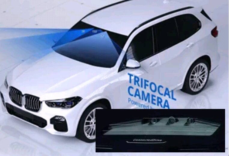
BMW X5 Equipped with Trino Camera
Taking the ZF S-Cam 3 monocular safety camera as an example, we can see that it has two main components: one is the processor board equipped with MobileEye EyeQ3, and the other is the board equipped with On Semiconductor’s CMOS image sensor (CIS).
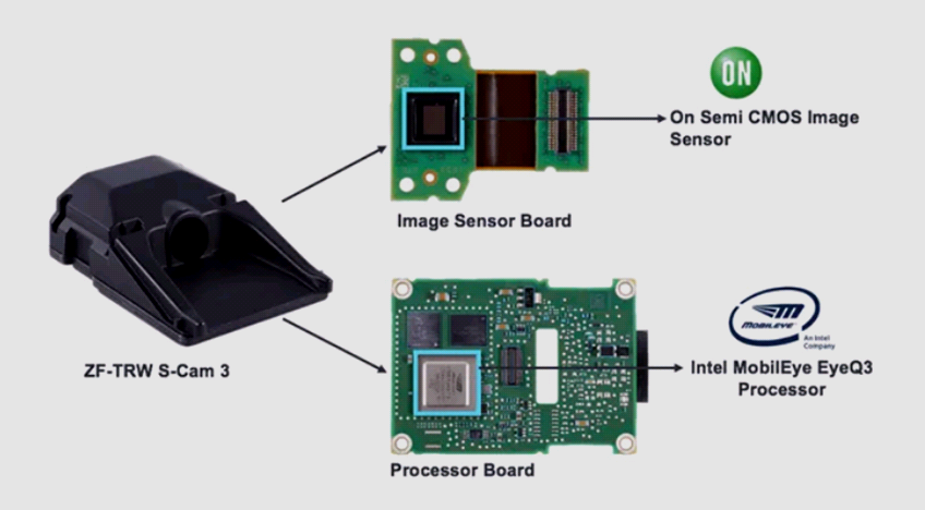
Monocular Camera Disassembly
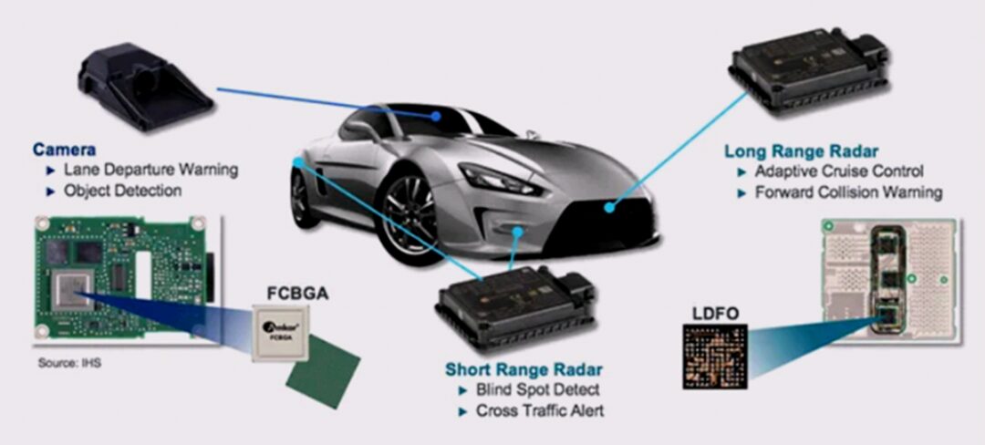
Another architecture uses multiple cameras around the vehicle, connecting them to a central wiring box. In the Tesla Model 3, there are 8 cameras around the vehicle, and their data is sent to the central ADAS control module located under the dashboard.
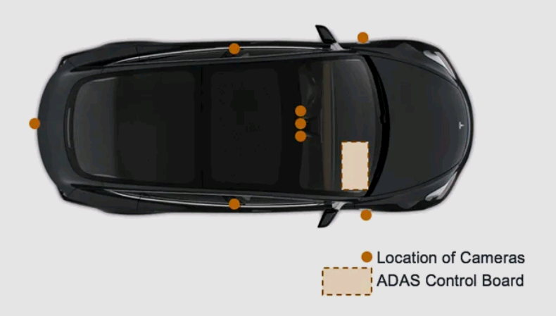
Camera and ADAS Control Board Location in Model 3
After years of development, the Tesla ADAS control board (i.e., Full Self-Driving (FSD) computer) HW3.0 uses two SoCs designed by Tesla and manufactured by Samsung using a 14nm process. This board contains many semiconductor devices. According to a report by IHS, the semiconductor content of HW2.5 is about $520.
Reportedly, the HW4.0 chip is jointly developed by Tesla and Broadcom and will be manufactured using TSMC’s 7nm process. It is expected to start mass production in the fourth quarter of 2021, with the first vehicles equipped with this chip expected to be delivered as early as the first quarter of 2022. The shift to TSMC for HW4.0 chip production is mainly due to its 7nm process, which can operate at a lower power supply voltage (below 500mV), achieving lower power consumption, and its performance is expected to be three times that of HW3.0.
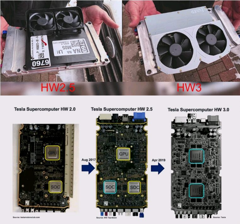
Evolution of Tesla HW
Another key component of the camera system is the CMOS image sensor. Most automotive camera modules use image sensors from On Semiconductor. In 2014, On Semiconductor acquired Aptina, which holds a strong position in the automotive industry, establishing a unique presence in the automotive CIS field.
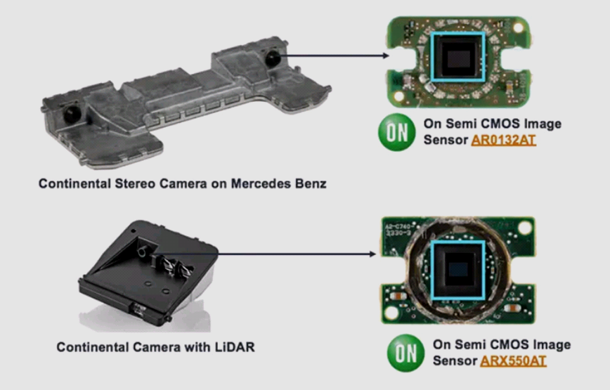
Continental Camera Module Using On Semiconductor Sensors
Another valuable ADAS function is blind spot monitoring. The radar module on the rear bumper enables this feature. Blind spot monitoring, also known as lane change assist, activates when the vehicle speed exceeds 10 km/h, continuously sending radar signals to the left and right 3 meters and 8 meters behind the vehicle, analyzing and processing the detected signals, filtering out fixed objects and distant objects. If a vehicle approaches within the detection area, the yellow light strip on the rearview mirror will flash as a warning.
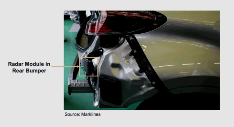
Blind Spot Monitoring Radar
There is also a long-range radar module at the front of the vehicle, supporting adaptive cruise control and automatic emergency braking. It may be installed in the vehicle’s front grille or front bumper, such as Mercedes’ millimeter-wave radar; BMW has cameras in addition to radar, while Audi A7 is equipped with both millimeter-wave radar and LiDAR.
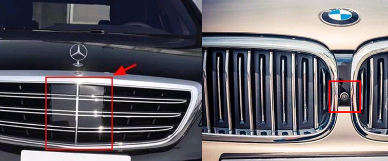
Forward Safety Monitoring of Mercedes and BMW
Continental’s long-range millimeter-wave radar module also has two boards: one is the processor board, and the other has the radar chip set and antennas, both equipped with NXP chips (MCU and transceiver, respectively).
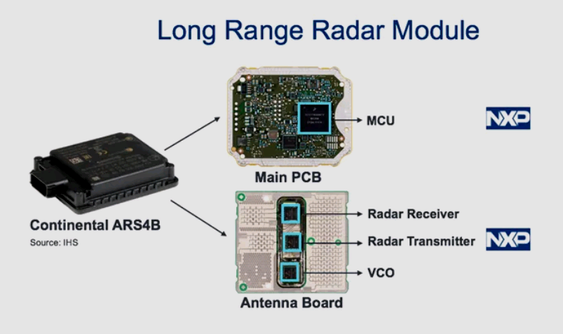
Disassembly of Millimeter-Wave Radar Module
In summary, the main functions of ADAS are realized by two systems in the vehicle:
Camera System: The CMOS image sensor captures images, which are processed by the processor. The processor uses flip-chip BGA (FCBGA) packaging.
Radar System: Typically, there are three radar modules in the vehicle. Two are on the rear bumper, and one is on the front grille. Each module has a transceiver for sending and receiving radar signals and a processor for processing radar signals. The radar transceiver uses LDFO packaging, and some use flip-chip CSP (FCCSP) packaging.
Until a few years ago, most semiconductor components in vehicles used wire bonding for packaging. Although wire bonding remains the mainstream packaging for automotive chips, ADAS modules are increasingly using advanced packaging, such as flip-chip FCBGA, low-density fan-out (LDFO), and flip-chip FCCSP.
Main ADAS Component Packaging Forms
Currently, whether for Autonomous Driving (ADS) or ADAS, vehicles must perform various driving functions under all conditions. To achieve this, vehicles must not only communicate with complex internal systems but also engage in more communication with the external environment. Future automotive technologies will continue to employ an increasing number of cameras, radars, and LiDARs. Sensor technology must become more robust, capable of handling more complex tasks. Automotive system components should provide higher performance to process more data at faster speeds while minimizing latency and power consumption. Therefore, finer nanotechnology has become a constant pursuit for semiconductor manufacturers. Depending on the functions of each automotive system, different processes are used.
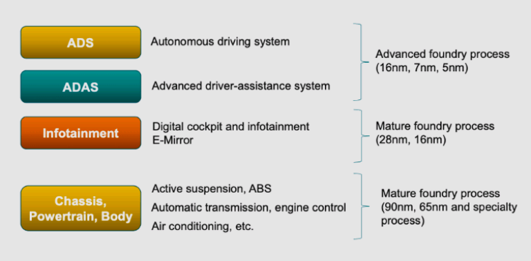
Process Technologies Used for Different In-Vehicle Functions
It is worth mentioning that although chip manufacturers have made every effort to keep up with Moore’s Law, progress is becoming increasingly difficult. Adopting advanced IC packaging technology has become a remedy that helps achieve scalability, functional density, and heterogeneous integration while reducing overall package size. Of course, automotive applications like ADAS will also benefit from this.
Driving Towards the Future
The development of ADAS has led to the widespread adoption of numerous driver assistance functions, continuously enhancing the overall driving experience, safety, comfort, and convenience. As analysts from Yole stated, entering the new decade, “ADAS is helping to climb the autonomous driving ladder defined by SAE in 2014, winning splendid performances with ‘L2’, ‘L2+’, and now ‘L2++’. But in terms of autonomous driving, reality may not be the same.” Nevertheless, the entire industry is accumulating more experience in achieving the highest level of automation for fully autonomous vehicles (AVs) during this process.

Scan to follow us
Beijing High-Level Autonomous Driving Demonstration Zone