Third generation semiconductors, also known as wide bandgap semiconductors, refer to semiconductor materials represented by gallium nitride (GaN) and silicon carbide (SiC), which can operate at higher temperatures, stronger voltages, and faster switching frequencies. They are suitable for fields such as smart grids, new energy vehicles, 5G communications, microwave RF, and deep space equipment.
The term third generation semiconductor is not entirely accurate; it does not simply replace the first and second generations but rather represents a complementary relationship, expanding the application of semiconductor materials in high-power and high-frequency domains.
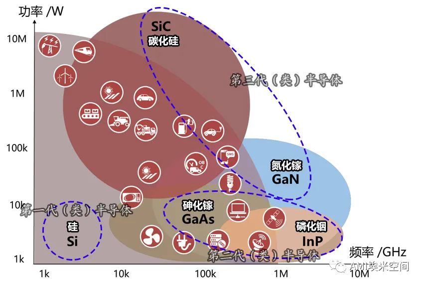
Power-frequency characteristics and application ranges of different semiconductor materials. Image source: Infineon
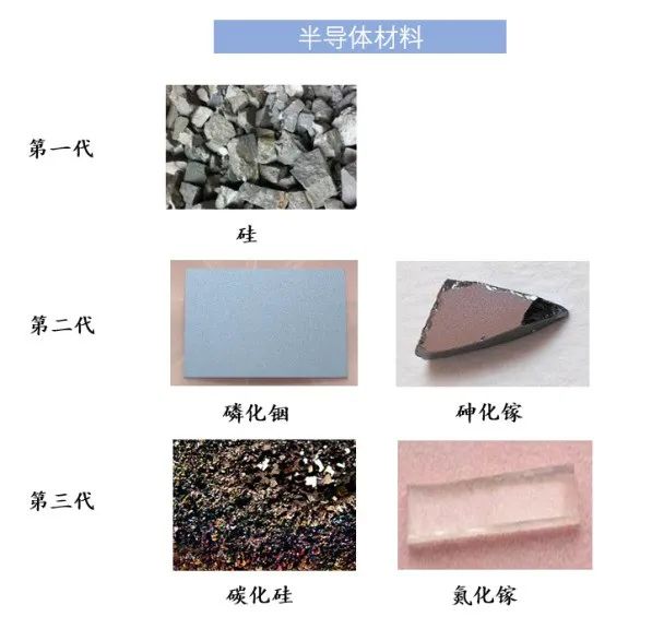
Images of semiconductor materials. Image source: Semiconductor Industry Observation
Third generation semiconductors include silicon carbide, gallium nitride, aluminum nitride, diamond, and zinc oxide. They are characterized by a wide bandgap, offering better electron mobility and the ability to withstand high temperature, high pressure, and high radiation environments.
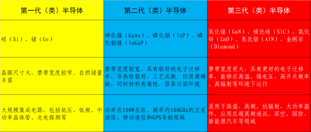
Comparison of first, second, and third generation (types of) semiconductors.
Currently, countries are still in a “race” phase regarding patent applications, standards, and scale for third generation semiconductors, with no complete monopoly observed. China maintains a strategic advantage in applications, markets, and certain technological fields, and various regions are accelerating the deployment of the third generation semiconductor industry. Presently, China is in a parallel state with international advanced levels in the field of optoelectronic materials and devices; the LED lighting industry has made significant progress and has become the first breakthrough point for China’s third generation semiconductor industry; however, in power electronic semiconductor materials and devices, as well as RF materials and devices, it is still in a following state compared to international advanced levels.
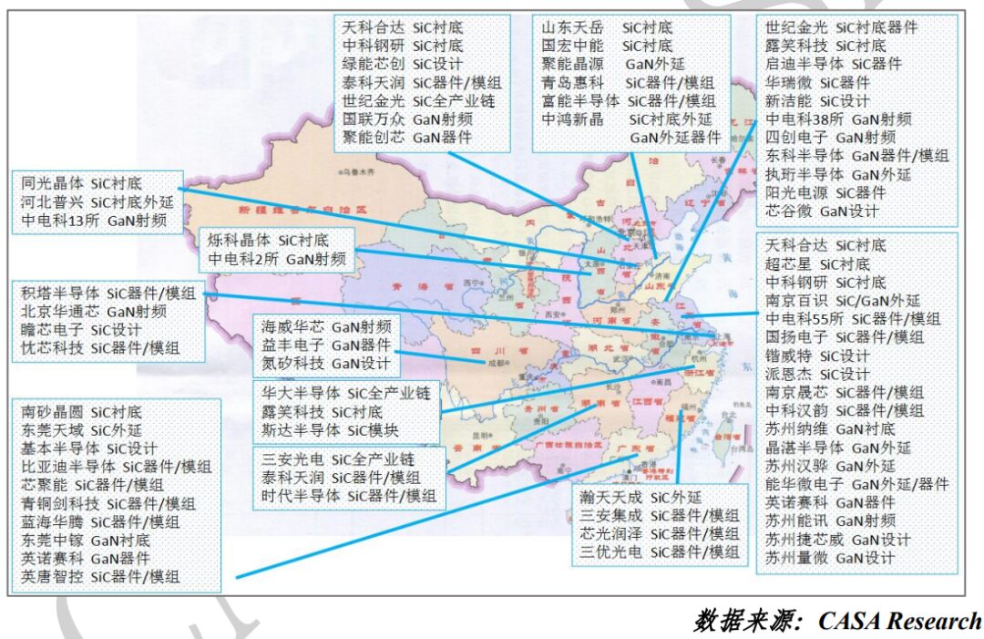
Distribution of some domestic third generation semiconductor projects. Image source: CASA Research
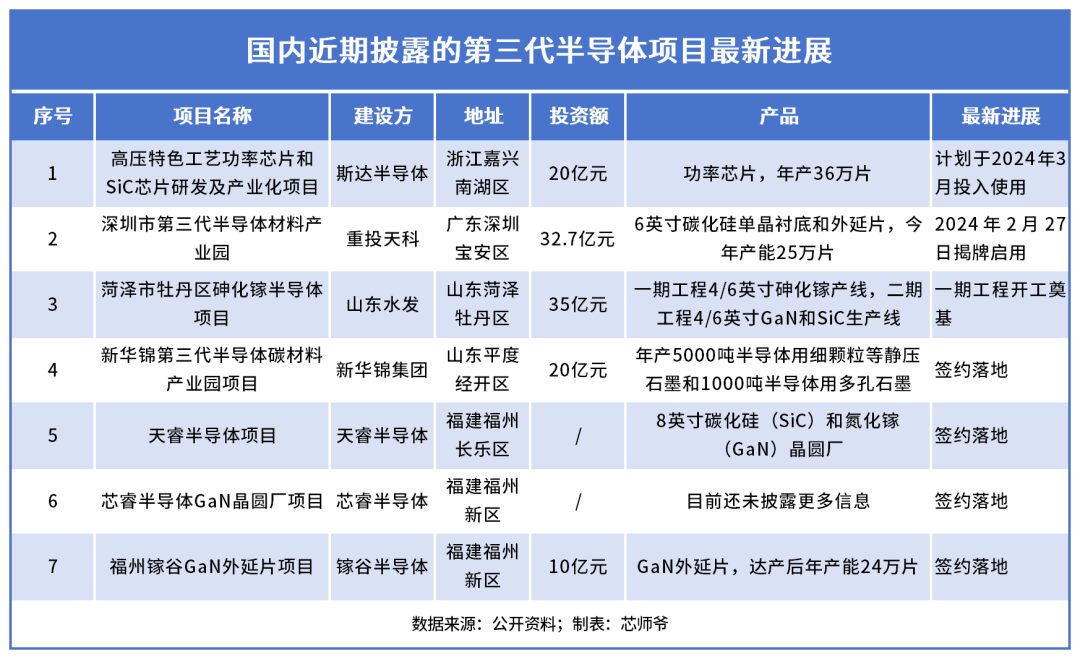
Progress of some domestic third generation semiconductor projects. Image source: Chip Master
Shenzhen’s third generation semiconductors excel in downstream applications, and the entire Greater Bay Area has a relatively complete supporting system. In February this year, Chongtou Tianke launched its third generation semiconductor silicon carbide material production base in Shiyan, Bao’an, with a total investment of 3.27 billion yuan, focusing on the layout of 6-inch silicon carbide single crystal substrate and epitaxy production lines, aiding Guangdong in creating a “third pole” for national integrated circuit industry development.
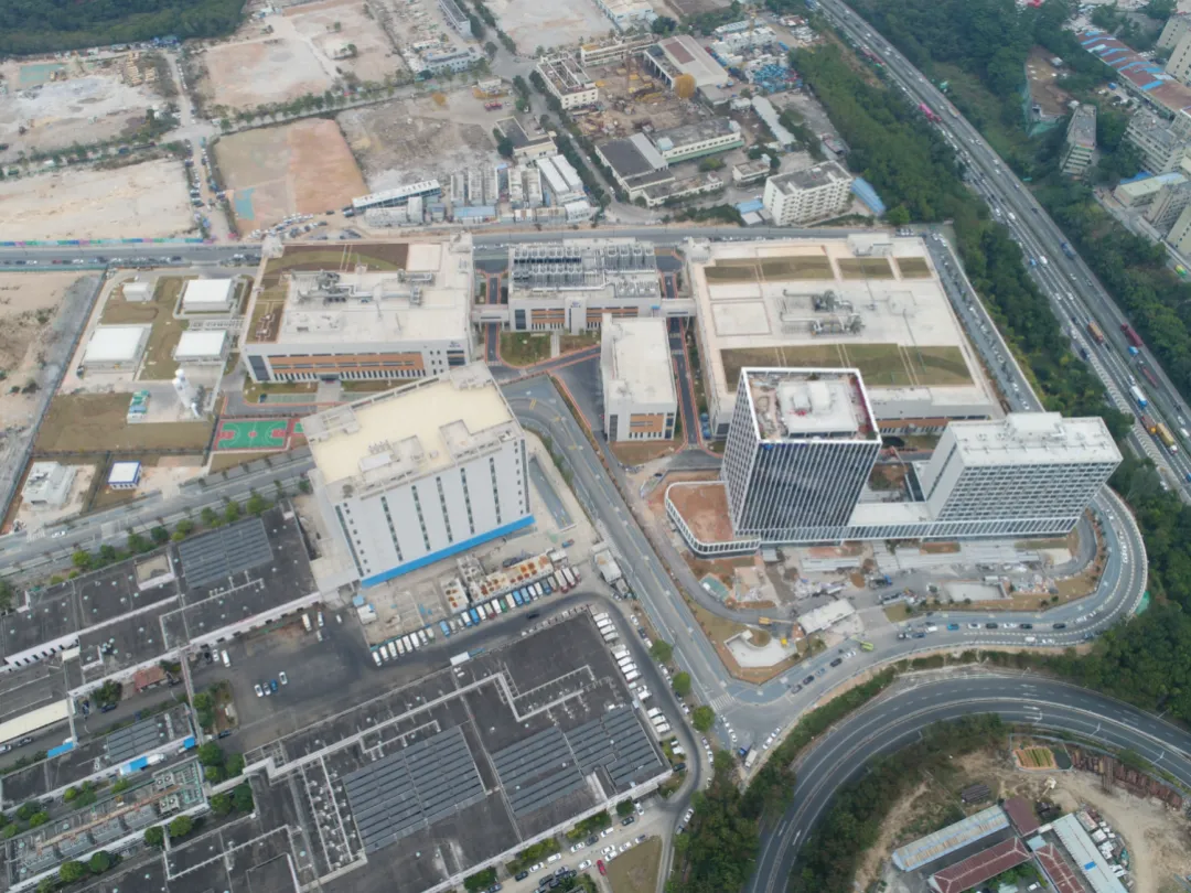
Chongtou Tianke third generation semiconductor industrial park. Image source: Bao’an Daily
In the realm of third generation semiconductors, if further classification is made, silicon carbide and gallium nitride are considered third generation, while aluminum nitride is viewed as 3.5 generations, and gallium oxide (Ga2O3), diamond, and zinc oxide are regarded as fourth generation. The fourth generation semiconductors, a concept proposed in the last 5-10 years, possess advantages such as “ultra-wide bandgap (4.2-4.9eV)”, “ultra-high critical breakdown field strength (8MV/cm)”, and “ultra-strong transparent conductivity”. Fourth generation semiconductors may become an important foundational support for the computing power era, driven by artificial intelligence and quantum computing in the future.
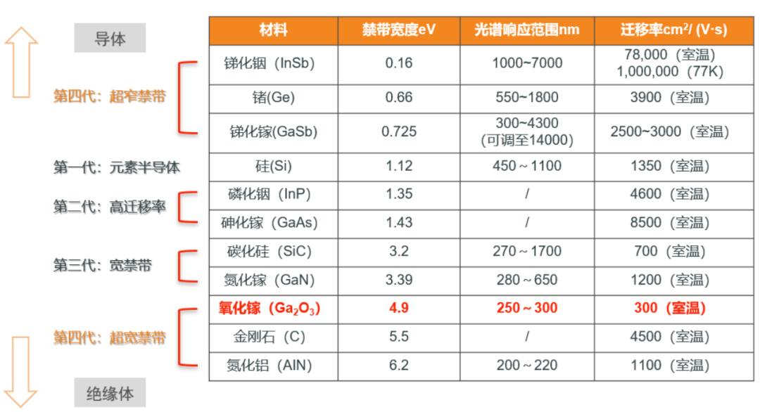
Comparison of parameters of different semiconductor materials. Image source: Eefocus