1Introduction to Circuit Boards
1. Flexible Printed Circuit Board
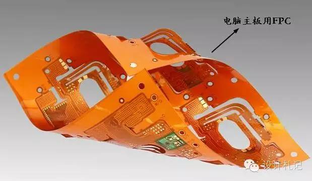
A flexible printed circuit board (Flex Print Circuit, abbreviated as “FPC”) is a printed circuit board made of flexible substrates, which can be single-sided, double-sided, or multi-layered. It features light weight, thinness, compactness, high density, high stability, and flexible structure. Besides static bending, it can also perform dynamic bending, curling, and folding.
2. Rigid Printed Circuit Board
A rigid printed circuit board (Printed Circuit Board, abbreviated as “PCB”) is made from rigid substrate materials that are not easily deformed. It remains flat during use. It has advantages such as high strength, resistance to warping, and secure installation of surface mount components.
3. Rigid-Flex Circuit Board
A rigid-flex circuit board (Rigid-Flex) is formed by selectively laminating rigid and flexible substrates together, creating a tight structure with metallized holes forming electrical connections. It features high density, fine lines, small hole diameters, compact size, light weight, and high reliability. Its performance remains stable under vibration, impact, and humid environments. It can be bent, installed in three dimensions, and effectively utilizes installation space, making it widely used in portable digital products such as mobile phones, digital cameras, and camcorders. Rigid-flex boards are increasingly used to reduce the footprint, especially in consumer electronics.
2Introduction to Circuit Board Materials
1. Conductive Medium: Copper (Cu)
﹣Copper Foil: Rolled Copper (RA), Electrolytic Copper (ED), High Ductility Electrolytic Copper (HTE)
﹣Thickness: 1/4OZ, 1/3OZ, 1/2OZ, 1OZ, 2OZ, these are common thicknesses
﹣OZ (ounce): unit of copper foil thickness; 1OZ = 1.4 mil
2. Insulating Layer: Polyimide (PI), Polyester, Polyethylene Naphthalate (PEN)
﹣The most commonly used is Polyimide (abbreviated as “PI”)
﹣PI Thickness: 1/2mil, 1mil, 2mil, these are common thicknesses
﹣1 mil = 0.0254mm = 25.4um = 1/1000 inch
3. Adhesive: Epoxy Resin, Acrylic.
﹣The most commonly used is epoxy resin, with thickness varying depending on different manufacturers.
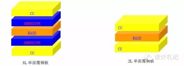
4. Copper Clad Laminate (Cuclad laminates, abbreviated as “CCL”):﹣Single-sided Copper Clad Laminate: 3LCCL (with adhesive), 2LCCL (without adhesive), as illustrated below.﹣Double-sided Copper Clad Laminate: 3LCCL (with adhesive), 2LCCL (without adhesive), as illustrated below.
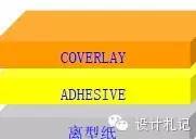
5. Covering Film (Coverlay, abbreviated as “CVL”): composed of insulating layer and adhesive, it covers the conductive lines to provide protection and insulation. The specific stacking structure is as follows.
2. Conductive Silver Foil: Electromagnetic Wave Protection Film
﹣Type: SF-PC6000 (black, 16um)
﹣Advantages: Ultra-thin, excellent sliding and bending properties, suitable for high-temperature reflow soldering, and good dimensional stability.
The commonly used is SF-PC6000, the stacking structure is as follows: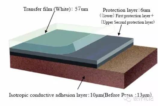
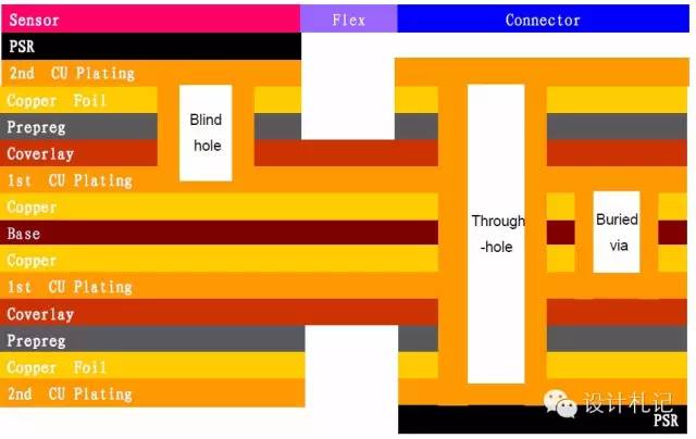
3Rigid-Flex Layer Structure Display
4Circuit Board Manufacturing Process
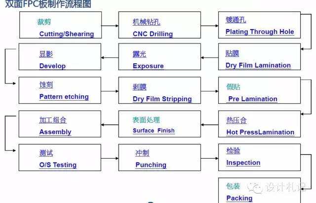
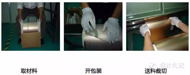
1. Material Preparation: Cutting
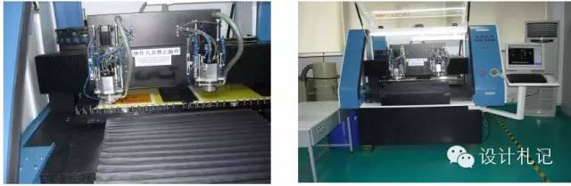
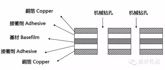
2. Mechanical Drilling
3. Plating Through Hole
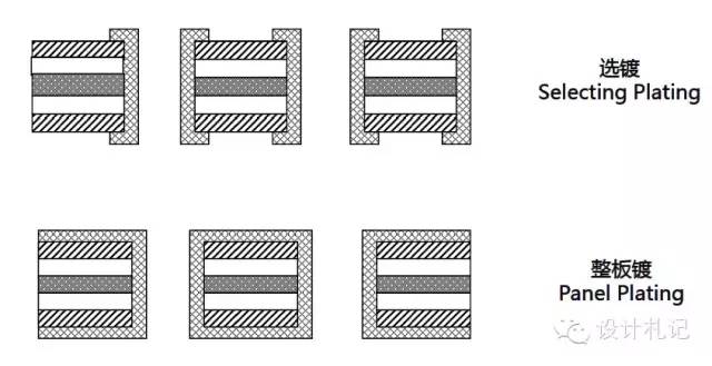
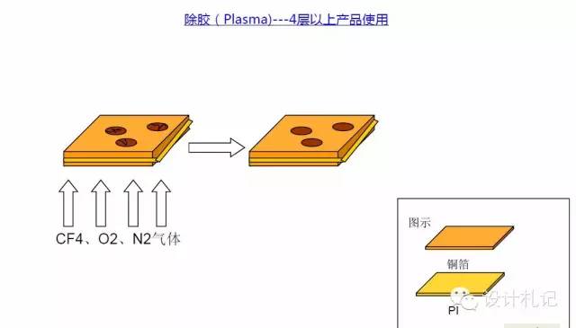
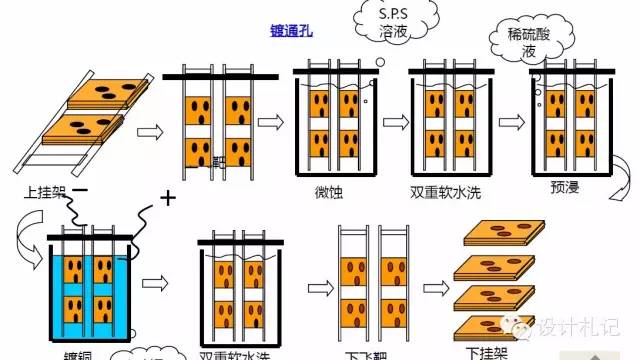
4. DES Process (Five Steps)
(1) Film Lamination (Dry Film Lamination)
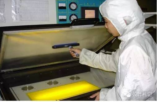
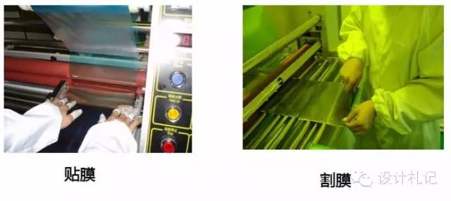 (2) Exposure
Working Environment: Yellow Light
Purpose: To create an optical polymerization reaction between the dry film and the transparent areas of the film through UV light exposure and the film mask. The areas where the film is brown cannot undergo optical polymerization due to UV light not penetrating.
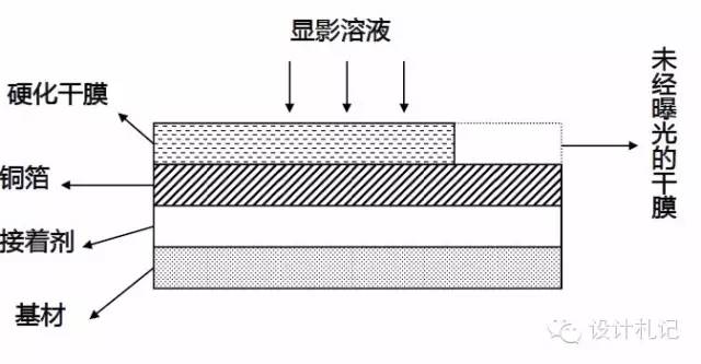
 (3) Development
Working Solution: Na2CO3 (K2CO3) Weak Alkaline Solution
Purpose: To wash away the undeveloped dry film areas using a weak alkaline solution.
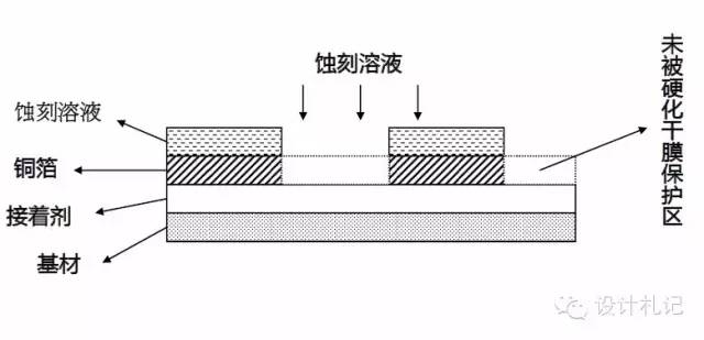
 (4) Etching
Working Solution: Acidic Water: HCl + H2O2
Purpose: To etch away the copper exposed after development using the chemical solution, forming the pattern transfer.
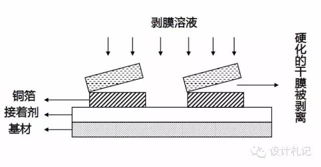
 (5) Film Stripping
Working Solution: NaOH Strong Alkaline Solution
5. AOI
Main Equipment: AOI, VRS System
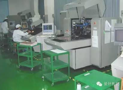
The formed copper foil lines must undergo scanning detection for line defects using the AOI system. Standard line image information is stored in data format in the AOI host, and the CCD optical camera scans the line information from the copper foil into the host for comparison with the stored standard data. If there are anomalies, the location will be numbered and recorded for transmission to the VRS host. The VRS magnifies the copper foil 300 times, displaying the defect locations sequentially based on prior records. Operators determine whether it is a true defect. True defects are marked with a water-based pen for easy classification and repair by subsequent workers. Workers use a 150x magnifying glass to assess defect types, form quality reports, and provide feedback to previous processes for timely improvement measures. Due to the fewer defects in single-sided boards and lower costs, manual inspection is preferred.
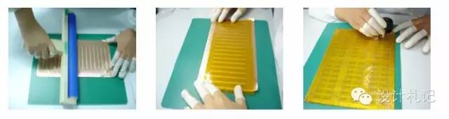
6. Dummy Paste
Protective Film Functions: 1) Insulation and anti-soldering; 2) Protecting the circuit; 3) Increasing the flexibility of flexible boards.
7. Hot Pressing
Working Conditions: High Temperature and High Pressure

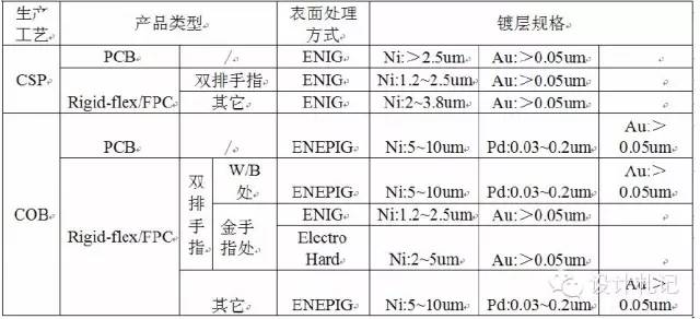
8. Surface Treatment
After hot pressing, surface treatment of the exposed copper foil areas is required.
The method is determined based on customer requirements.
9. Screen Printing
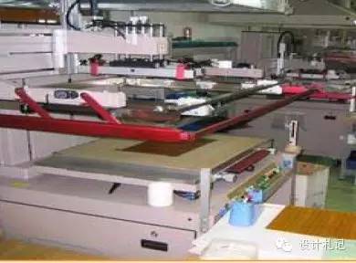
Main Equipment: Screen Printer, Oven, UV Dryer. The screen printing equipment transfers ink onto the product through the screen printing principle. It primarily prints product batch numbers, production cycles, texts, black masks, and simple circuit layouts. The product is aligned with the screen using positioning pins, and ink is pressed onto the product using a squeegee. The screen is open for text and pattern sections, while non-text or pattern sections are sealed with photosensitive emulsion, preventing ink leakage. After printing, the product enters the oven for drying, and the printed text or pattern layer tightly bonds to the product surface. Some special products require specific circuits, such as adding a few circuits to a single-sided board to achieve double-sided board functionality, or adding a shielding layer to a double-sided board, which must be achieved through printing. If the ink is UV-drying ink, a UV dryer must be used. Common issues include ink leakage, contamination, gaps, bulging, and peeling.
10. Testing (O/S Testing)
Testing fixtures + testing software perform full functional inspection of the circuit board.

11. Punching
Corresponding shape molds: knife molds, laser cutting, etched molds, simple steel molds, steel molds.

12. Assembly
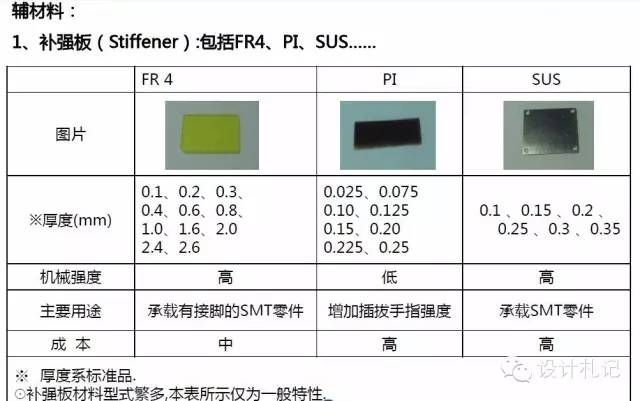
Assembly refers to assembling materials according to customer requirements. Suppliers can provide:
A. Stainless Steel Reinforcement
B. Beryllium Copper Sheets/Phosphor Bronze Sheets/Nickel-Plated Steel Sheets Reinforcement
C. FR4 Reinforcement
D. PI Reinforcement
13. Inspection
Inspection Items: Appearance, Dimensions, Reliability
Testing Tools: Two-Dimensional Measuring Instrument, Micrometer, Caliper, Magnifying Glass, Soldering Furnace, Tension Tester

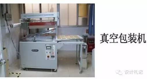
14. Packaging
Packaging Methods: 1. Plastic Bag + Cardboard
2. Low Adhesion Packaging Material
3. Standard Vacuum Box
4. Special Vacuum Box (Anti-Static Grade)
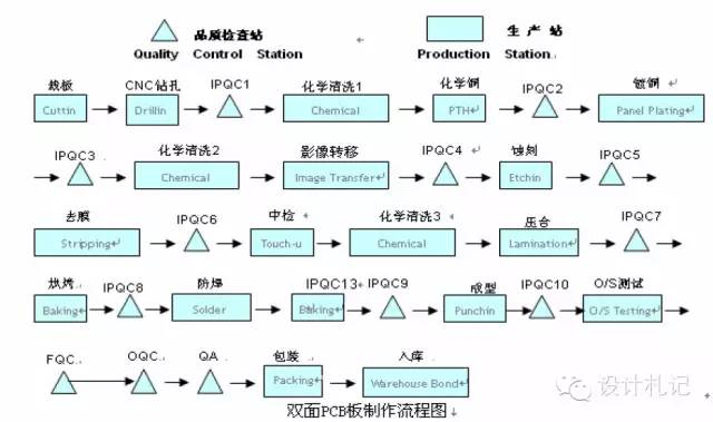
 Double-Sided PCB Manufacturing Process Diagram
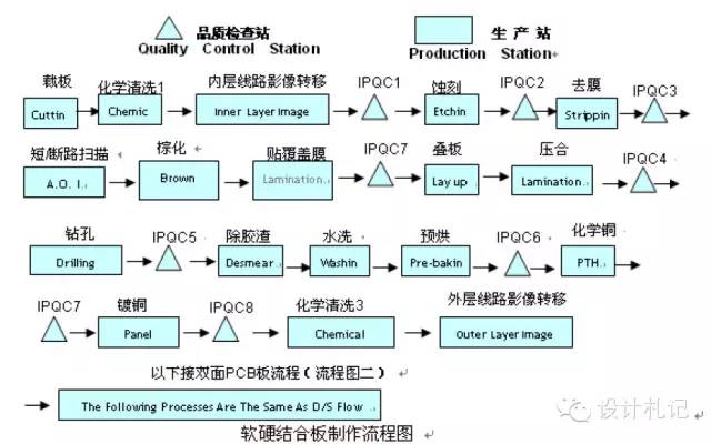
Rigid-Flex Board Manufacturing Process Diagram
5Circuit Board Case Sharing
1. Design Proposal
1. Proposal Description:
• New COF proposal integrates reinforcement and chip attachment area onto a single steel sheet, as shown in the FPC schematic.
• Main Uses:
• 1. To minimize the sensor’s contact with uneven circuit board surfaces, directly attaching the sensor to a flat steel sheet surface, making the sensor perpendicular to the optical axis of the lens, reducing image blurriness.
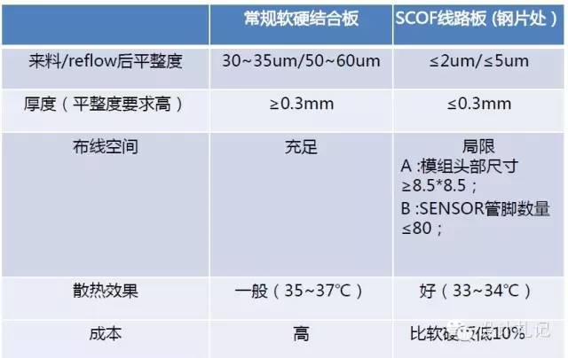
• 2. In the ≤0.3mm proposal, the new COF’s flatness outperforms rigid-flex boards, achieving a lower module height while ensuring flatness.
• 3. Direct contact between the sensor and steel sheet enhances thermal conductivity.

2. Design Proposal
1). P8V12G-621-00 Circuit Board (Structural Diagram Below):
Design thickness of the circuit board is 0.3mm, with a steel sheet protrusion height of 0.02mm.
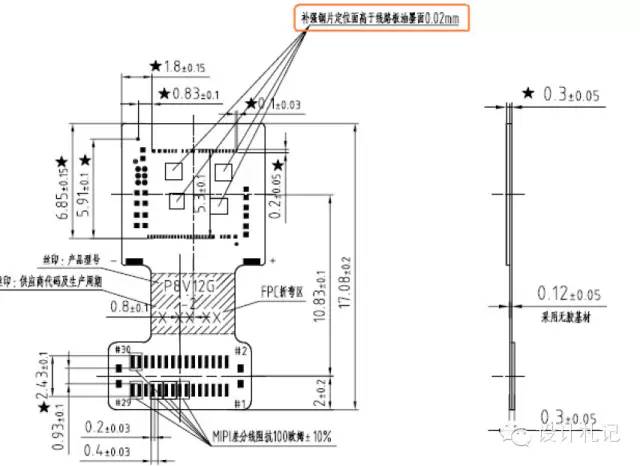
2). P8V12G-621-00 Circuit Board (Wiring Diagram Below):
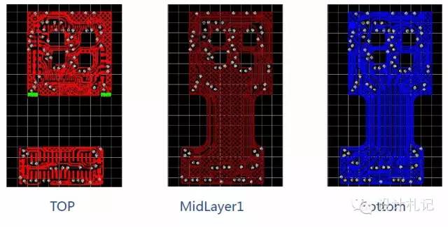
3). P8V12G-621-00 Circuit Board (Layer Structure Diagram Below):
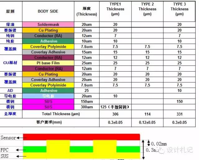
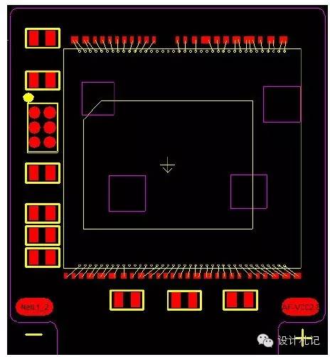
4). Limitations of Circuit Board Design Evaluation:
1. The purple small box in the diagram indicates the steel sheet support area;
2. The support area is distributed diagonally across the SENSOR;
3. The minimum window area of the support area is 0.5*0.5; larger areas yield better flatness;
4. Module head dimensions ≥8.5*8.5;
5. SENSOR pin count ≤80;
6. MIPI 2 Lane output is more advantageous for routing compared to 4 Lane output;
7. MIPI positioned near the connector is more favorable for routing (as shown in the right diagram, MIPI routing is below the pad);
3. Advantages and Disadvantages Comparison Analysis
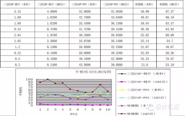
4. Flatness Data Comparison:
Comparison of flatness under different types for P8V12G:
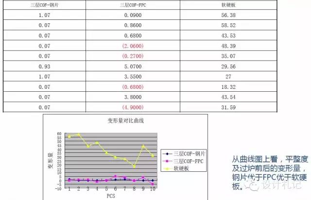
Comparison of flatness deformation before and after furnace passing for P8V12G under different types:
Disclaimer: The publication of this article is intended to convey more information. If there are errors in source attribution or infringement of your legitimate rights, please contact the author with proof of ownership, and we will promptly correct or delete it. Thank you.