0. Introduction
1. Overview of SWD
SWD stands for Serial Wire Debug, which translates to “串行线调试” in Chinese. SWD is one of the two debug ports currently supported by ARM, the other being the JTAG Debug Port, which is the debug port commonly used on J-link (in JTAG mode). Based on the ARM CoreSight debugging architecture, SWD can read and write the chip’s registers by transmitting data packets. SWD is a two-wire protocol used to access the ARM debug interface. It is part of the ARM Debug Interface Architecture Specification and serves as a replacement for JTAG. The physical layer of SWD consists of two lines:
SWDIO: Bidirectional data line
SWCLK: Host-driven clock line
The following diagram is a simple connection diagram of SWD:
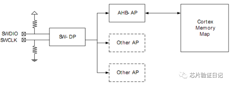
External devices (such as debug probes) can directly access the Serial Wire Debug Port (SW-DP) by connecting to SWDIO/SWCLK. SW-DP can access one or more Access Ports (AP), through which the remaining registers of the system can be accessed. An important AP for the Cortex M series CPU is the AHB-AP, which is the host on the internal AHB bus. In other words, the AHB-AP can access the memory map of the internal core. Since the internal flash, SRAM, debug components, and peripherals are all memory-mapped, the AHB-AP can control the entire device, including programming it. The entire SWD operation process is hierarchical, with the clock signal input from the SWCLK pin and the data signal input/output from the SWDIO pin. First, the Debugger operates on the SW-DP to determine the parameters of the AP registers, enabling operations on the Cortex Memory Map.
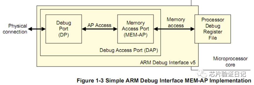
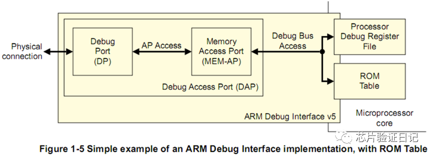
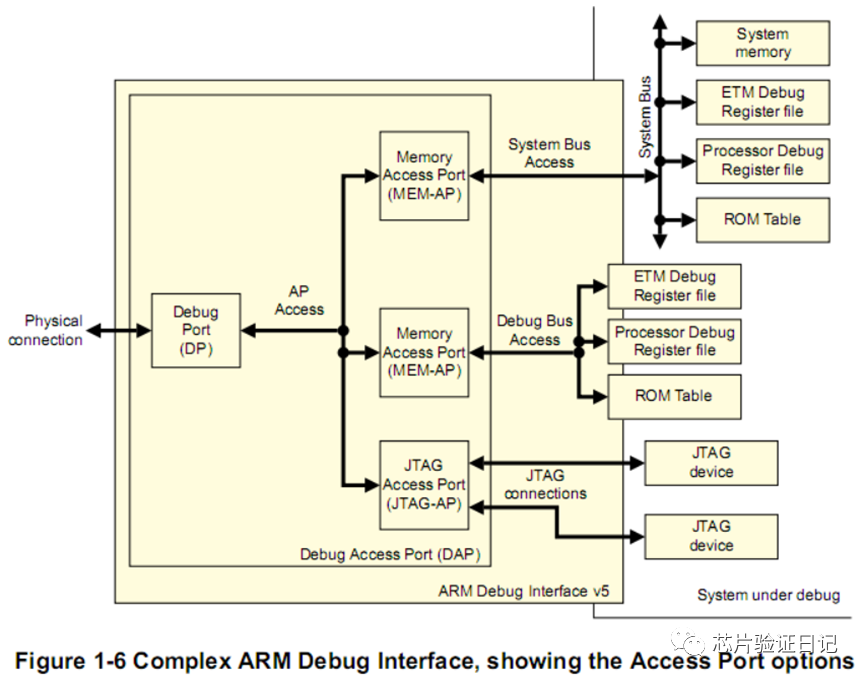
The following three screenshots illustrate the connection implementation of the ARM Debug Interface. As shown in the figure, the DAP consists of two parts: DP and MEM-AP (commonly referred to as AP). MEM-AP is a general term, encompassing APB/AHB/AXI-AP.
2. SWD Protocol
2.1 SWD Commands
2.1.1 Host Sends Packet Request
The external host debugger sends a request to the DP, which is the target of this request.
The request sent by the host consists of 8 bits, as shown in the figure below:
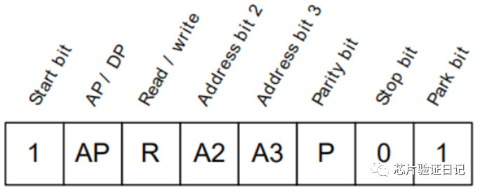
Bit0: Start, fixed to 1.
Bit1: APnDP, 0 indicates access to DP registers, 1 indicates access to MEM-AP registers.
Bit2: RnW, 0 indicates a write request, 1 indicates a read request.
Bit[4:3]: Address value A[3:2], storing the address of the DP/AP registers.
Bit5: Parity, used to indicate the total number of odd bits in {APnDP, RnW, A[2:3]}.
Bit6: Stop, fixed to 0.
Bit7: Park, fixed to 1.
2.1.2 Target Returns ACK
The ACK value returned by the target consists of 3 bits: ACK[0:2]==001 indicates FAULT, ACK[0:2]==010 indicates WAIT, ACK[0:2]==100 indicates OK response.
2.1.3 Data Bit Transmission
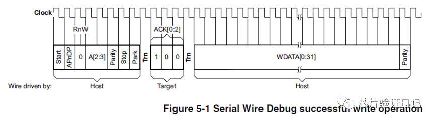
Data consists of 32 bits of valid data + 1 bit of parity bit.
2.2 DAP Registers
During SWD communication, the main registers involved are two: one DP (Debug Port) and one AP (Access Port). To access the core registers, the access sequence is DP -> AP -> Core Register.
2.2.1 DP Registers
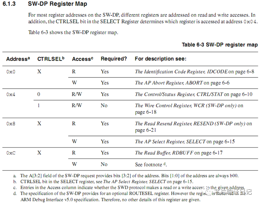
The DP registers are shown in the figure below, with the address indicated by ADDR[2:3] in the packet header. For details, please refer to the “ARM Debug Interface v5 Architecture Specification”.
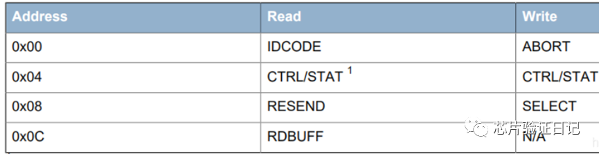
The following diagram is a table created by a netizen based on ADI5’s description, which is easier to understand.
IDCODE Register
IDCODE: Identification Code Register, used to identify SW-DP. The IDCODE register provides identification information about SW-DP. On devices with Cortex-M3 or Cortex-M4 cores, this register should be 0x2BA01477. For devices with Cortex-M0+ cores, this register should be 0x0BC11477.
ABORT Register
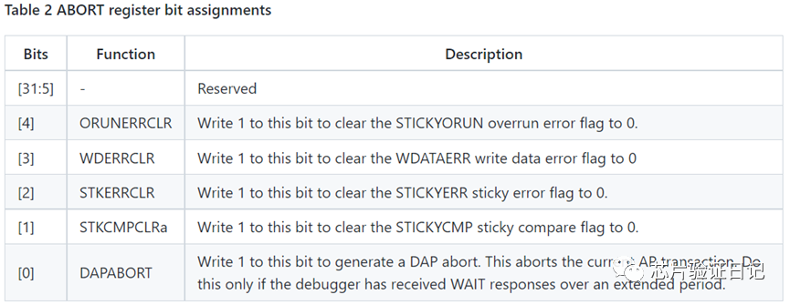
ABORT: Abort register, forces AP transactions to abort. During communication, if a sticky error occurs at position 1 (ack = 4). Writing 0b1 to ABORT will generate a DAP abort, forcing the current AP transaction to abort.
The main purpose of the ABORT register is to force the DAP to abort, and on SW-DP, it is also used to clear error and sticky flag conditions. Below is the definition of each bit of the AP ABORT register.
CTRL/STAT Register
RDBUFF Register
RDBUFF: Read Buffer Register, on SW-DP, RDBUFF shows the data captured during the last AP read, allowing repeated return values without generating a new AP access.
It is worth noting that after a bus reset, it is necessary to perform a switch operation between JTAG and SWD (send 0x79E7 or 0xE79E), then you must read the IDCODE first to determine the type of MCU before continuing with other operations.
2.2.2 AP (MEM-AP) Registers
MEM-AP provides DAP access to the memory subsystem. Since memory, peripherals, and debug components are all memory-mapped, MEM-AP can be used for programming and debugging Cortex M0/M3, etc.
Compared to DP registers, AP registers are much more complex. For details, please refer to the “ARM Debug Interface v5 Architecture Specification”.
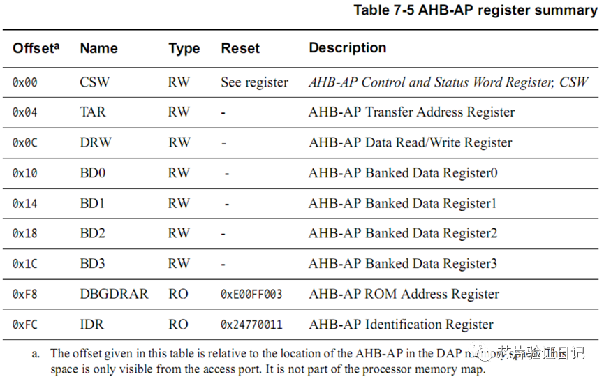
The following diagram is a table created by a netizen based on ADI5’s description, which is easier to understand.
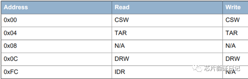
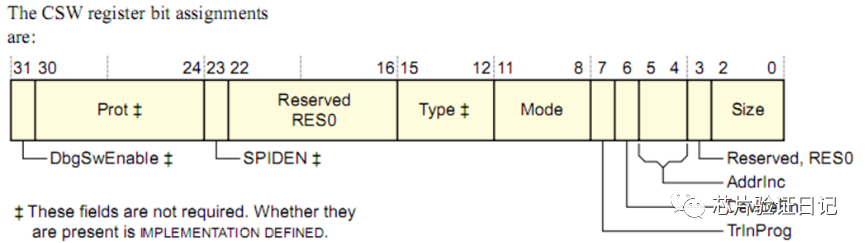
CSW Register
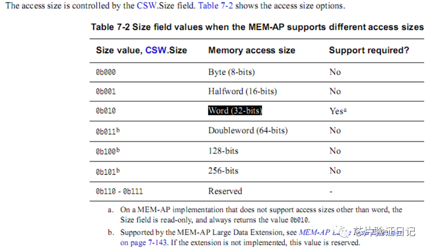
CSW: Control/Status Word Register, CSW configures and controls the memory system accessed through MEM-AP. size: 32bit-0b010; 16bit-0b001
TAR Register
TAR Register: Transfer Address Register, saves the memory address to be accessed. By setting b01 in the AddrInc field of the CSW register, the content of TAR can be automatically incremented upon successful access to DRW.
DRW Register
DRW: Data Read/Write Register, used to write or read data from the address specified in TAR. DRW directly maps the value passed in the AP access to one or more memory accesses at the address specified in TAR. When intending to write a value to a memory address, the address is first written to the TAR register, and then the value is written to DRW. When intending to read data from a memory address, the address is first written to TAR, and then the value is read from DRW.
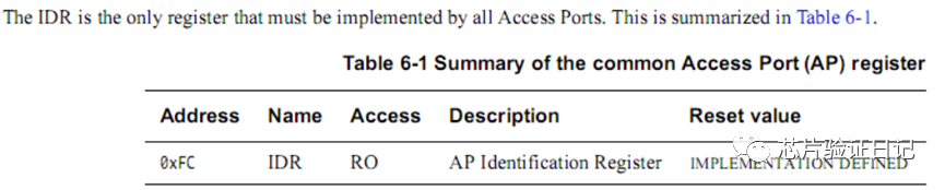
IDR: Identification Register, IDR identifies the accessed port. To read this register, the APBANKSEL field should be set to 0xF. The IDR register can then be read using address 0x0C (ADDR[3:2]=b11). For devices with Cortex-M3 or Cortex-M4 cores, the IDR register should return the value 0x24770011. For devices with Cortex-M0+, it should return 0x0477003.
2.3 Debug and System Registers
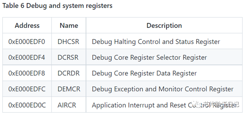
The following screenshot shows the Cortex M3 debug registers. Using the debug registers, we can set the Core to halt mode and change Core registers such as SP or PC.
2.3.1 DHCSR Register
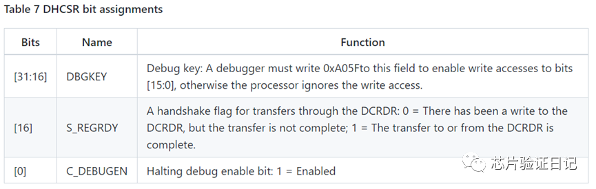
DHCSR=Debug Halting Control and Status Register
DHCSR controls the processor’s halt, single-step, and restart actions. When C_DEBUGEN is set to 1, halt debugging will be enabled. For more detailed information, please refer to the “ARM Cortex-Mx Authority Guide”.
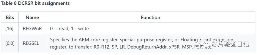
2.3.2 DCRSR
DCRSR register = Debug Core Register Selector Register, provides debug access to the ARM core registers, special-purpose registers, and Floating-point extension registers. A write to DCRSR specifies the register to transfer.
2.3.3 DCRDR
Debug Core Register Data Register, DCRDR register provides debug access to the ARM core registers, special-purpose registers, and floating-point extension registers. DCRDR is the data register for these accesses.
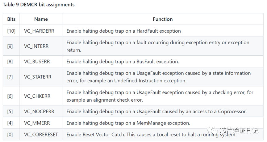
2.3.4 DEMCR
Debug Exception and Monitor Control Register, DEMCR register manages vector catch
behavior and DebugMonitor handling when debugging. Bits [23:16] provide DebugMonitor exception control. Bits [15:0] provide Debug state, halting debug, control.
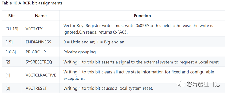
2.3.5 AIRCR
Application Interrupt and Reset Control Register, AIRCR register sets or returns interrupt control data.
2.4 SWD Protocol Operation Timing
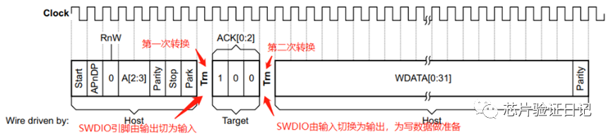
2.4.1 Successful Write Timing
As shown in the figure below, it is worth noting the trn (turnaround period), because we are using single-bus communication, where both write and read occur on the same line, and this trn occurs during the delay when switching from write to read.
2.3.2 Successful Read Timing
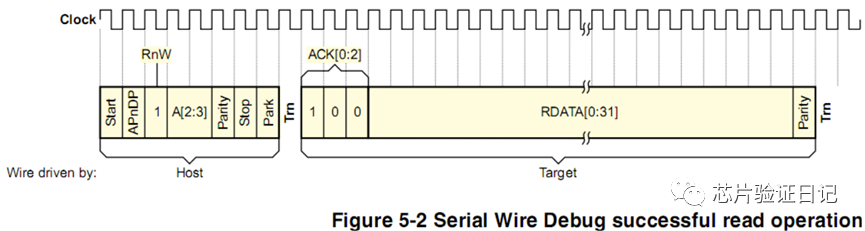
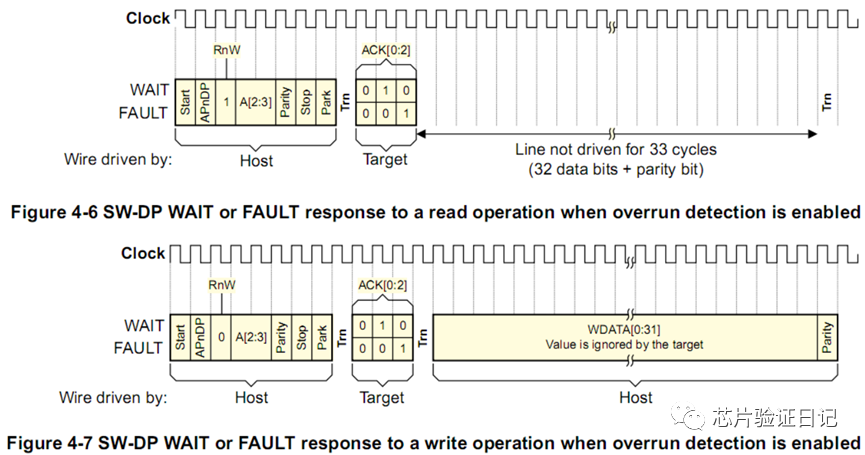
2.3.3 Response WAIT Timing
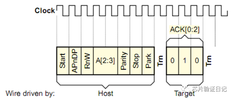
2.3.4 Response FAULT Timing
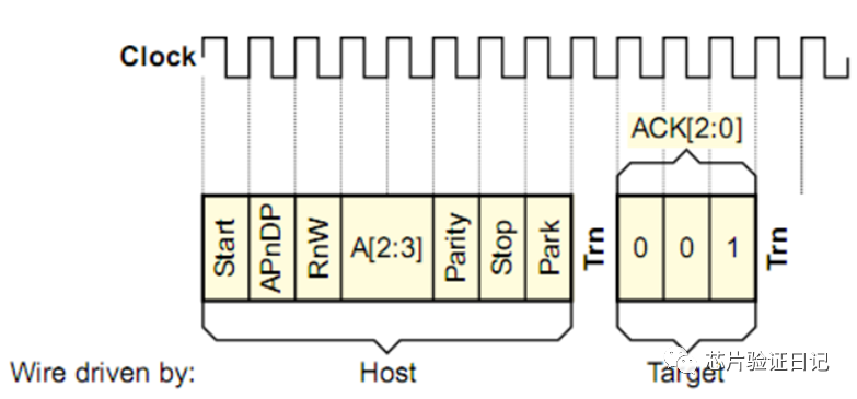
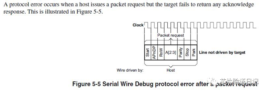
2.3.5 Protocol Error Response
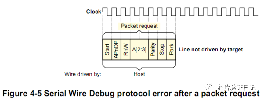
2.3.6 Sticky Overrun Behavior
3. SWD Operation Steps
3.1 SWD Initialization Steps
-
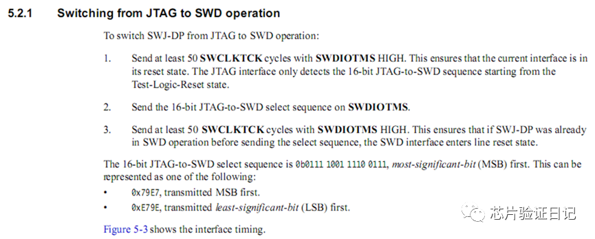
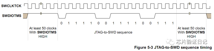
a) InitializeIO ports, set SWCLK and SWIO to output mode, keep SWDIO=1, ensuring that Host continuously sends at least 50 “1”, allowing Target to perform a Line Reset. -
b) Send JTAG to SWD command, 0x79E7 two bytes, then send a line reset operation again. -
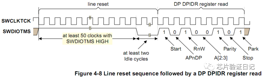
c) Send at least two Idle signals, keeping SWDIO=0. -
d) Read the chip’s IDCODE, completing the SWD initialization operation. At this point, only the DP register group can be accessed, while the AP register group is still inaccessible. Note that after a reset, the IDCODE must be read once (located in DP register). Set the address to 00b, and read the DP operation to read the IDCODE, which varies depending on the core model; mine is 0x0BB11477.
3.2 Accessing AP Registers via DP
-
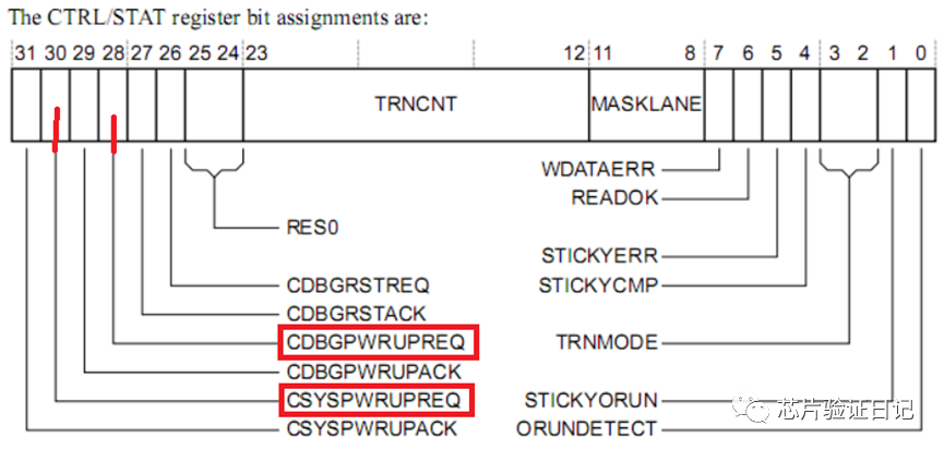
1) Write 0x50000000 to the CTRL/STAT register in DP (bits 28 and 30), enabling the debug port and its clock;
CSYSPWRUPREQ: System powerup request; CDBGPWRUPREQ: Debug powerup request
-
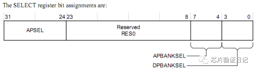
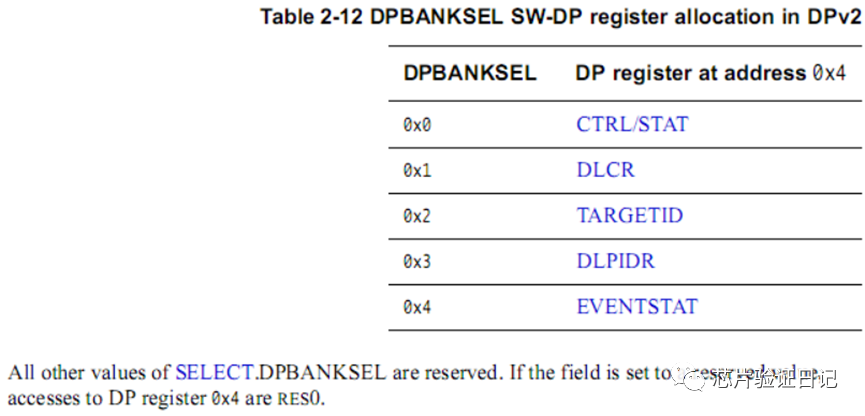
2) Write to the SELECT register in DP to determine APBANK.
3) Read the data from the IDR register (addr = 0xFC) and verify it
4) Write 0x00000002 to the CSW register, data_size: 32bit
3.3 Read/Write Operations
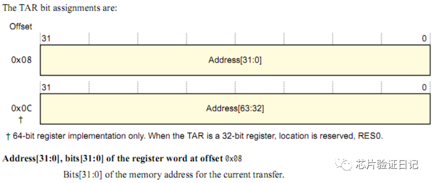
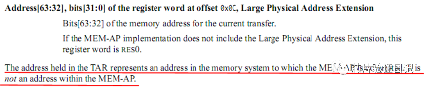
The screenshot above explains clearly that the address in the TAR register is not the address inside the AP, but the physical address in the chip system connected to the AP.
DRW register directly maps the AP access to one or more memory accesses inside the chip system. The AP access will not complete until the memory access is finished.
DRW register is R/W (readable and writable), and its offset in the MEM-AP register space is 0x0C.
In write mode, DRW writes the currently transmitted value to the address specified in TAR.
In read mode, DRW holds the current transmitted value read from the address specified in TAR.
3.2.1 Write Operation
3.2.2 Read Operation
3.4 Notes During Read/Write:
Due to the special nature of reading AP registers, the returned data is the value from the last transmission. In other words, there are two ways to obtain the correct value of the AP register.
a) Send the read operation for the DRW register twice;
b) Send one read operation for the DRW register (reading the data from the previous cycle), then send one read operation for the RDBUFF register (reading the data you need)
In general, reading/writing DP registers has no latency and does not require two reads/writes. Reading AP registers has latency; the first time reading AP gets the previous cycle’s value, and the second time reading AP gets the desired value. Writing AP registers has no latency. For TAR and DRW, writing once is sufficient.
4. Programming SRAM via SWD
This section will demonstrate step-by-step how to program the internal SRAM via SWD.
4.1 Initialization
-
a) Send more than 50 cycles of SWCLK/TCK, SWDIO/TMS=1. This ensures that both SWD and JTAG are in a reset state. -
b) Send the 16-bit JTAG-to-SWD select sequence on SWDIOTMS -
c) Send more than 50 cycles of SWCLK/TCK, SWDIO/TMS=1. This ensures that if SWJ-DP is already in SWD mode, SWD will perform a line reset before sending the select sequence. -
d) Perform READID to verify that SW-DP has switched to SWD operation.
4.2 Halt CPU
Before programming the internal SRAM or FLASH, the CPU should first be reset and halted. This is mainly to set the CPU and peripherals to a known state and prevent the CPU from inadvertently running part of the code while programming.
The specific operation steps are as follows,
a)Write 0xA05F0001 to DHCSR, which enables halt debug.
b)Write 0x01 to DEMCR. This enables Reset Vector Catch.
c)Write 0xFA050004 to AIRCR. This resets the core.
Now, the core will halt at the first instruction, and all peripherals and registers (except debug registers) will be set to reset values.
4.3 Memory and Core Register Access.
4.3.1 Access Memory
-
a) Set 32 bit width and auto increment in CSW register.
-
b) Write memory address in TAR register
-
c) Access DRW register for read/write data.
4.3.2 Access Core Registers
Read:
-
b) Write DCRSR address into TAR register.
-
c) Write core register index Rn into DRW register.
-
d) Write DCRDR address into TAR register.
-
e) Read core register value from DRW register.
Write:
5 Notes During SWD Operations
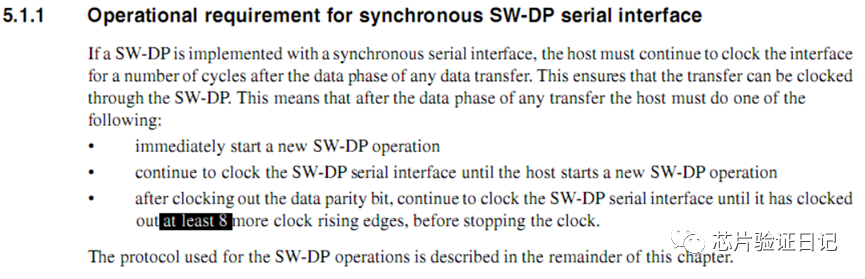
5.1 Additional 8 Cycles of Clock After Data Transmission Completion
5.2 Errors in Invalid Request Packets
5.3 Write Data Error WDATAERR
5.4 STIKYERR
The possible reasons are: the Debug power domain has been powered down; or there was an error with the debug resources (e.g., core error); or there is a problem with the corresponding design logic;
Once this error is detected, debugging must be done carefully, modify the code, and then reconnect.
Writing articles is not easy. If you find this helpful, please give a thumbs up or treat me to a chicken leg!