With the rapid development of the digital age, the global demand for high-speed data transmission continues to rise, and silicon photonic technology has become one of the key solutions to this challenge.
Silicon photonic technology utilizes silicon materials as a foundation, integrating the processing of optical signals and electronic signals on a single chip, achieving not only high-performance data transmission but also significantly reducing power consumption and costs.
From the expansion of data centers to high-performance computing (HPC) fields, and the upgrading of telecommunications networks, silicon photonic technology is changing the way modern communication and data transmission operate with its irreplaceable advantages.
The application range of silicon photonic technology is extensive, playing an indispensable role especially in data centers and telecommunications networks.In data centers, silicon photonic technology can significantly enhance the data interconnection speed between servers while reducing heat generation, achieving more efficient energy use.
In telecommunications networks, silicon photonic technology supports the upgrade of fiber optic communication, providing stable long-distance high-bandwidth signal transmission to meet the demands of the future 5G and cloud computing era.
Looking ahead, the market potential of silicon photonic technology is limitless, and it is expected to continue playing a crucial role in high-speed data transmission, artificial intelligence, and quantum computing.
In this context, the performance of APD (Avalanche Photodiode) and PD (Photodiode), which are core components in silicon photonic systems, directly affects the overall system performance, becoming a key factor that cannot be ignored in the development of silicon photonic technology.

The Architecture of Silicon Photonic Technology: The Synergistic Effect of Light Emission, Waveguides, and Light Reception

The core architecture of silicon photonic technology consists of three main functional modules: light emission, waveguides, and light reception. These modules work together to support high-speed, low-power optical communication systems, interlinked to form an efficient optical signal processing system.
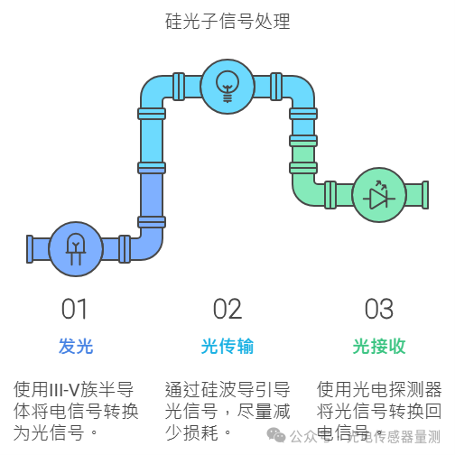
1. Light Emission:The light emission module is primarily responsible for converting electrical signals into optical signals. Since silicon is an indirect bandgap semiconductor, its light emission efficiency is relatively low, making it difficult to achieve efficient light sources directly.
Therefore, modern silicon photonic technology typically employs lasers made from III-V semiconductor materials (such as Gallium Arsenide GaAs or Indium Phosphide InP) as light sources, connecting them to silicon-based optical paths through heterogeneous integration or external coupling.
This hybrid integration scheme can fully utilize the excellent light emission efficiency of III-V materials while maintaining compatibility with silicon-based processes.2. Waveguides:The waveguide is the key channel for optical signal transmission in silicon photonic technology, guiding optical signals from the light emission module to the light reception module. In practical applications, the transmission loss of silicon waveguides mainly comes from several aspects:• Scattering Loss:Primarily caused by the roughness of the waveguide sidewalls, which can be reduced by optimizing etching processes and surface treatment techniques.• Absorption Loss:Includes intrinsic absorption of the material and free carrier absorption, which can be optimized through doping concentration control and region design.• Bending Loss:Radiation loss generated at waveguide bends, which can be minimized through reasonable bend radius design. To reduce these losses, modern silicon waveguide manufacturing employs various optimization techniques, such as silicon dioxide cladding technology and sidewall smoothing treatments, allowing transmission losses to be controlled at levels of 0.1-0.3 dB/cm.
Thanks to the low loss characteristics of silicon materials and the maturity of manufacturing processes, silicon waveguides can transmit multi-wavelength optical signals with extremely high efficiency while also offering small size and high integration advantages.
However, in long-distance transmission, the attenuation of optical signal strength and multimode interference still need to be optimized.3. Light Reception:The core link of photoelectric conversion, the light reception module is responsible for converting the optical signals transmitted in the waveguide into processable electrical signals, making it a key terminal in silicon photonic systems.
The main components are photodetectors, such as APD and PD. The efficiency and stability of light reception not only directly affect signal quality but also determine the overall system’s reliability and data transmission rate.
APD (Avalanche Photodiode) is a highly sensitive photodetector that utilizes the built-in avalanche multiplication effect to achieve efficient amplification of optical signals under low light conditions.
Its working principle is based on the electron-hole pairs generated by photon absorption. When photons enter the APD, the photon energy is absorbed within the semiconductor material, generating free electrons and holes.Under high reverse bias, these initial carriers further trigger a collision ionization process, leading to the excitation of more carriers, ultimately achieving multi-stage amplification of the signal, which is the core of the avalanche multiplication effect.During this process, the ionization coefficient is an important parameter that characterizes the ability of carriers to generate new electron-hole pairs.The ratio of the ionization coefficients of electrons and holes (k value) directly affects the noise characteristics of the APD, with a smaller k value being favorable for obtaining a lower excess noise factor.To optimize the performance of the APD, modern devices commonly adopt a reach-through structure design. This structure includes independent absorption, multiplication, and transport layers, offering the following advantages:
• Achieving spatial separation of light absorption and carrier multiplication processes.
• Obtaining a more uniform electric field distribution, improving multiplication efficiency.
• Reducing dark current, enhancing signal-to-noise ratio.
• Improving response speed and broadening frequency response.
The main advantages of APD lie in its extremely high sensitivity and fast response time, making it particularly suitable for scenarios requiring precise optical signal detection, such as fiber optic communication and LiDAR applications.
In these high-demand applications, APD can effectively enhance signal reception capability and reduce signal loss during transmission.
PD (Photodiode) is a simple structure but widely used photodetector, whose working principle is based on the photoelectric effect. When photons incident on the PD exceed the bandgap energy of the material, electron-hole pairs are generated, producing photocurrent under the influence of the built-in electric field.
PD is mainly used to convert optical signals into electrical signals and is an important component in the photoelectric conversion process.
PD plays a significant role in various application scenarios, including optical communication, optical sensors, and photovoltaic devices.
Compared to APD, PD has a simpler structure and lower operating voltage, making it suitable for most applications with moderate sensitivity requirements.
However, when it comes to high-speed data transmission or weak light detection, APD becomes the more ideal choice due to its high gain characteristics.
The Role of APD and PD in Silicon Photonic ROSA
ROSA (Receiver Optical Sub-Assembly) is a core component in silicon photonic systems, primarily responsible for converting optical signals into electrical signals for efficient data transmission.
Its basic structure includes optical components (such as coupling lenses and filters), photoelectric conversion devices (such as APD or PD), and circuit modules for amplifying and processing the converted electrical signals.
In modern high-speed data transmission applications, ROSA plays a key role in signal reception and processing, directly affecting the performance of the entire system.
The Key Role of APD and PD in ROSA In the ROSA module, APD and PD are the core components executing photoelectric conversion, and their performance directly determines the signal reception efficiency and quality.
APD, with its high sensitivity and built-in gain function, is particularly suitable for applications requiring high signal-to-noise ratios and low light power detection, such as long-distance fiber optic communication and data transmission under weak light conditions.
On the other hand, PD, due to its low power consumption and high response speed, shows advantages in short-distance communication and cost-sensitive applications.
However, as data transmission rates continue to increase, the performance bottlenecks of ROSA modules gradually become apparent, especially under high-frequency and high-bandwidth demands, where the efficiency and stability of photoelectric conversion components become key challenges determining overall system performance.
Therefore, precise testing and optimization of the performance of APD and PD have become an indispensable part of the silicon photonic industry. In silicon photonic ROSA modules, the performance of APD and PD directly affects data transmission rates, signal quality, and system reliability.
For example, high external quantum efficiency (EQE) and excellent spectral response can ensure efficient conversion of optical signals across a multi-wavelength range, while low noise equivalent power (NEP) and high detectivity (D*) can enhance signal sensitivity and accuracy.
At the same time, stable I-V characteristics help improve the performance of components under different operating conditions, ensuring stable system operation.
Why is Light Reception Performance Key to Silicon Photonic Technology?
In silicon photonic systems, light reception performance is crucial because it is the final step in the entire signal transmission link.
The efficiency of the light reception module determines whether optical signals can be accurately and completely converted into electrical signals, directly affecting the reliability and speed of data transmission.
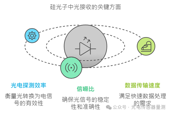
1. The Importance of Photoelectric Conversion Efficiency In the light reception module, external quantum efficiency (EQE) is the core indicator for measuring photoelectric conversion performance.High EQE means that more incident photons are effectively converted into current, thereby reducing signal loss and improving communication efficiency.
2. Challenges of Signal-to-Noise Ratio and Sensitivity APD and PD must possess excellent signal-to-noise ratios and sensitivity under low light intensity or high-frequency transmission conditions, which directly affects the stability and accuracy of optical signals.Low noise equivalent power (NEP) and high detectivity (D*) are key to enhancing signal quality.
3. Demand for High-Speed Data Transmission In modern silicon photonic applications, the increase in data transmission rates places higher demands on light reception performance.For example, in data centers and 5G communications, light reception modules need to have fast response and high-frequency bandwidth characteristics to meet the challenges of large data volume transmission.
Key Parameters Affecting APD and PD Performance
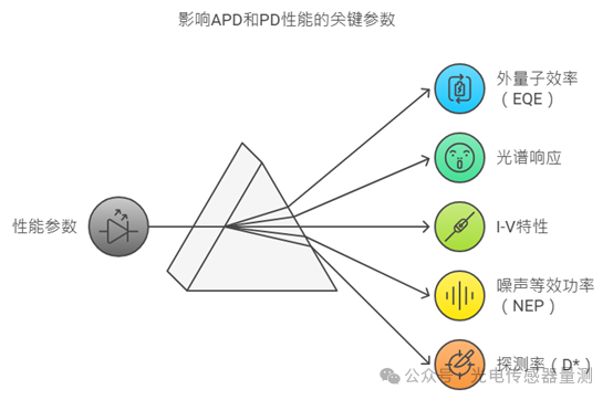
External Quantum Efficiency (EQE) External Quantum Efficiency (EQE) is one of the important indicators for evaluating the performance of photodetectors, representing the ratio of the number of incident photons to the number of generated electrons.For APD and PD, high EQE means higher photoelectric conversion efficiency, capable of producing larger current output under the same optical power.EQE spectral measurements can help research and optimize the material selection and structural design of devices, such as improving response efficiency within specific wavelength ranges to meet the multi-wavelength application needs of silicon photonic systems.Spectral Responsivity Spectral responsivity reflects the sensitivity of photodetectors at different wavelengths and is a key parameter for converting photon energy into current.In silicon photonic technology, the bandwidth range and uniformity of spectral responsivity directly affect the reliability and stability of data transmission. Through precise spectral responsivity measurements, bandwidth design can be optimized to enhance device performance in high-speed communication while ensuring compatibility in multi-wavelength operating environments.I-V Curve The I-V curve (current-voltage characteristic curve) reveals the electrical performance of photodetectors, including dark current, linear response range, and saturation characteristics.In APD, the I-V curve can also reflect the operational state of the avalanche multiplication effect, thus assessing its gain and noise performance. By testing the I-V curve under different light intensities, the impact of light intensity on output current can be studied, further analyzing non-linear effects and device stability.Additionally, testing the constant current or voltage over time can provide data support for transient response and long-term stability.NEP (Noise Equivalent Power) NEP (Noise Equivalent Power) describes the sensitivity of photodetectors, indicating the minimum optical power required when the detected signal equals the noise power.Noise equivalent power (NEP) is related to the device’s responsivity (R) and dark current (Id) as follows: NEP = (2qId)^(1/2) / R, where q is the charge of an electron. A lower NEP value indicates higher detection sensitivity.For applications requiring high sensitivity, such as weak light detection or long-distance fiber optic communication, low NEP is a key indicator of superior performance for APD and PD.Through NEP spectral measurements, noise sources can be identified, and effective structural or material improvements can be made to enhance signal-to-noise ratio and detection efficiency.
Detectivity (D*) Detectivity (D*) is an important parameter for comprehensively evaluating the performance of photodetectors, considering factors such as sensitivity and bandwidth.Detectivity D is related to the effective area (A) of the device and bandwidth (Δf): D = (A·Δf)^(1/2) / NEP. This indicates that under the same NEP conditions, a larger detection area can achieve a higher D* value.However, in practical applications, a trade-off must be made between detection area and response speed. High D* indicates that the device has higher limit detection capability and lower background noise interference, which is crucial for the application of APD and PD in silicon photonic systems.D* spectral measurements can help designers optimize structures and expand the application range of devices to meet more stringent usage conditions. The above key parameters are not only important indicators for measuring the performance of APD and PD but also the core basis for optimizing and improving the application of silicon photonic technology.By accurately measuring these parameters, scientific support can be provided for the research and production of photodetectors, further enhancing the overall performance of silicon photonic systems.This is also the core issue that Enlitech’s APD-QE testing equipment focuses on, providing comprehensive and efficient testing solutions for the industry.
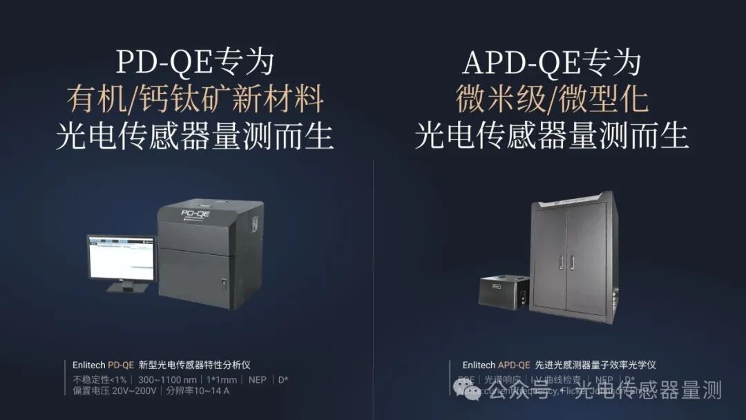
APD-QE Advanced Optical Sensor Quantum Efficiency Optical Instrument –Enlitech Technology
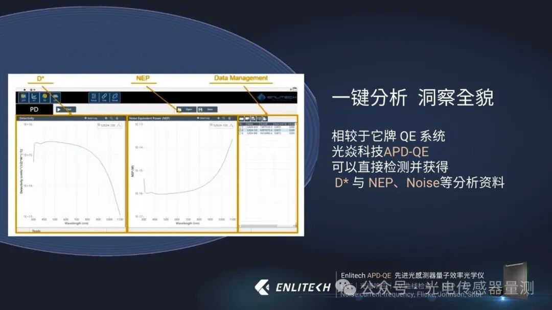
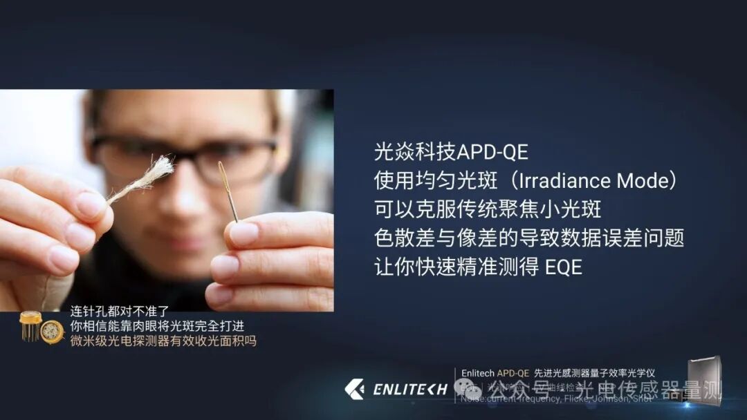
A. Comprehensive Coverage of Key Performance Parameter Measurements The APD-QE system employs a unique beam spatial uniformity technology, using the “Irradiance Mode” that complies with ASTM E1021 standards for testing, replacing traditional focused small spot methods.This design allows for accurate measurement of key parameters such as external quantum efficiency (EQE), spectral responsivity (SR), I-V curves, noise equivalent power (NEP), and detectivity (D*) of micron-level photodetectors, providing a one-stop solution for comprehensive performance evaluation of APD and PD.At the same time, this design significantly enhances testing accuracy and reproducibility, effectively reducing testing time and costs, meeting diverse needs in research and production.
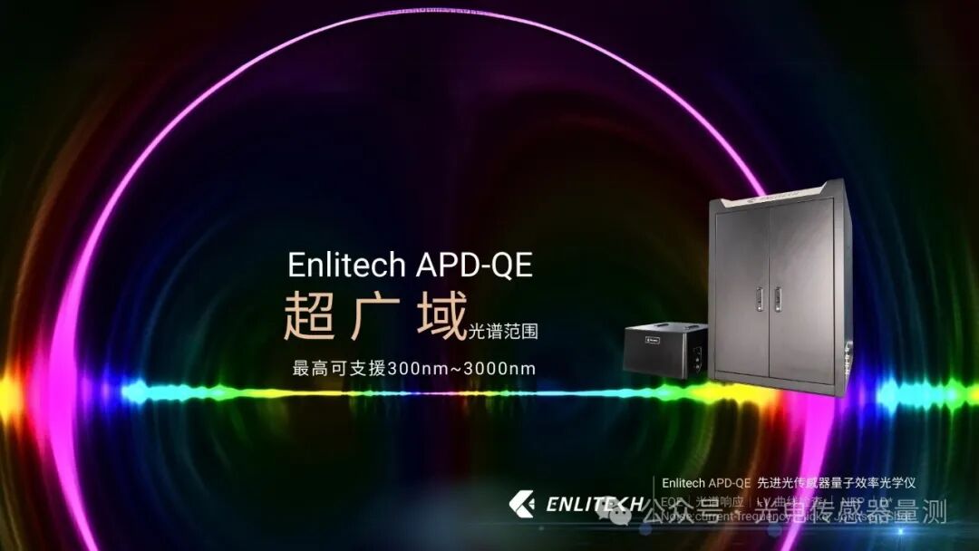
B. High Precision and Reliability Testing Capability The APD-QE is equipped with a highly stable light source and precision optical modules, capable of high-resolution spectral measurements from ultraviolet to near-infrared ranges (300nm~3000nm).
Its built-in light source modulation technology ensures high reproducibility of test data, providing consistent and accurate results even across multiple tests and different samples.Additionally, the device is validated according to ASTM standards, ensuring that test results have internationally recognized authority, meeting the stringent accuracy requirements of the silicon photonic industry and providing strong technical support for research and industrial applications in silicon photonics.
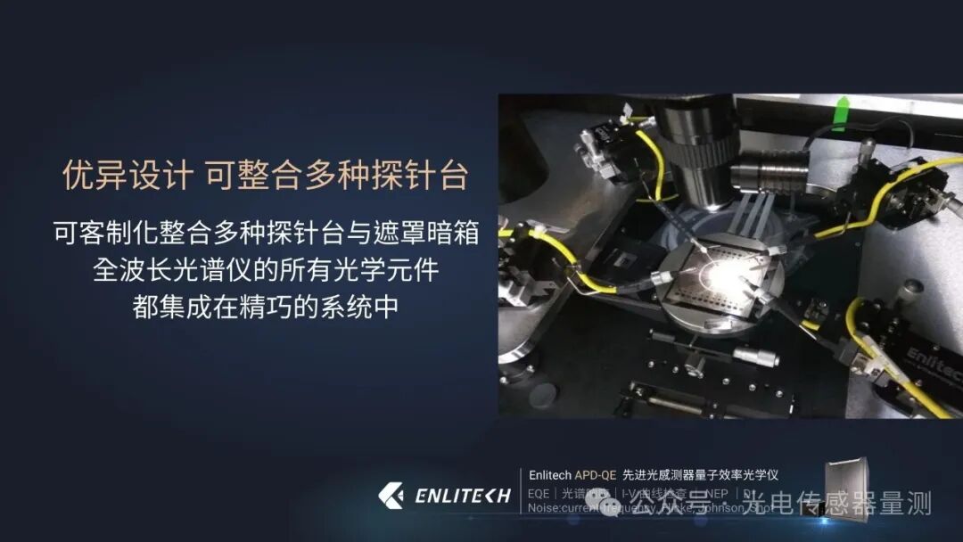
C. Benefits for APD and PD Research and Production The APD-QE system can be paired with various probe station systems to achieve non-destructive rapid testing, integrating optical and testing systems to improve system setup efficiency.
These features not only accelerate the R&D cycle of APD and PD but also enhance quality control levels, ensuring excellent performance of products in silicon photonic applications.
The comprehensive testing capabilities of APD-QE can effectively accelerate the R&D cycle of APD and PD.
By obtaining precise test data in real-time, researchers can quickly adjust material selection or structural design, validate the feasibility of innovative technologies, and ensure that product performance reaches optimal levels, thereby enhancing market competitiveness.
D. Value Created for the Silicon Photonic Industry The APD-QE is not only an efficient testing device but also an important tool for promoting the development of silicon photonic technology.Through its excellent testing capabilities, APD-QE supports the rapid development of new APD and PD, facilitating the verification and implementation of innovative designs.At the same time, it provides key support for optimizing the performance of light reception modules (ROSA), ensuring reliability and efficiency in high-speed data transmission.More importantly, APD-QE plays a significant role in promoting standardization in the silicon photonic industry and supporting academic research and industry collaboration.Enlitech’s APD-QE is not only an efficient testing device but also a key tool for driving technological progress.Its comprehensive, precise, and efficient testing capabilities provide strong support for the application of APD and PD in the silicon photonic industry.With the powerful functions of APD-QE, researchers and manufacturers can stand out in fierce market competition, driving innovation and development in silicon photonic technology.As silicon photonic technology continues to expand in applications such as high-speed data transmission, cloud computing, and telecommunications networks, the importance of APD (Avalanche Photodiode) and PD (Photodiode) as core components of photoelectric conversion becomes increasingly significant.
The performance of these components not only directly affects the efficiency and stability of light reception modules (ROSA) but also determines the operational quality of the entire silicon photonic system.
Key parameters such as external quantum efficiency (EQE), spectral responsivity (SR), noise equivalent power (NEP), and detectivity (D*) are core indicators for evaluating the performance of these components and are the technical foundation for driving breakthroughs in silicon photonic technology.Enlitech’s APD-QE testing equipment, with its comprehensive performance parameter testing, high precision testing capabilities, and multiple support for R&D and production, has become an indispensable technical tool in the silicon photonic industry.It not only provides researchers with verification means for innovative designs but also offers manufacturers efficient quality control support. As an advanced testing device that meets international standards, APD-QE lays a solid foundation for the application and commercialization of silicon photonic technology, helping the industry maintain a competitive edge in the international market.As key components in silicon photonic technology, the performance testing of APD and PD is an important link in driving the entire industry forward.Enlitech’s APD-QE provides precise and comprehensive solutions for this critical link, supporting both scientific innovation and enhancing the market competitiveness of enterprises.In the future, on the development path of silicon photonic technology, APD-QE will continue to play an irreplaceable role, becoming a solid backing for technological progress and industrial development.
For more technical discussions and support, please contact Enlitech Technology Enlitech
Email:[email protected]
Phone:+86-21-31338780/ 4001009282