
1
Silicon carbide has excellent performance, and the substrate is the most critical link
After decades of development, the performance of traditional silicon (Si) material devices has gradually approached the limits of silicon materials, with limited room for performance improvement. Modern power electronics technology has higher requirements for semiconductor materials in terms of high temperature, high voltage, and high frequency. Silicon carbide (SiC), a compound semiconductor material composed of silicon and carbon, is a typical representative of third-generation compound semiconductors. Compared to the first generation dominated by silicon and the second generation dominated by gallium arsenide, silicon carbide has advantages such as a wide bandgap, high saturation electron drift rate, and high thermal conductivity.
Comparison of first, second, and third generation semiconductor materials
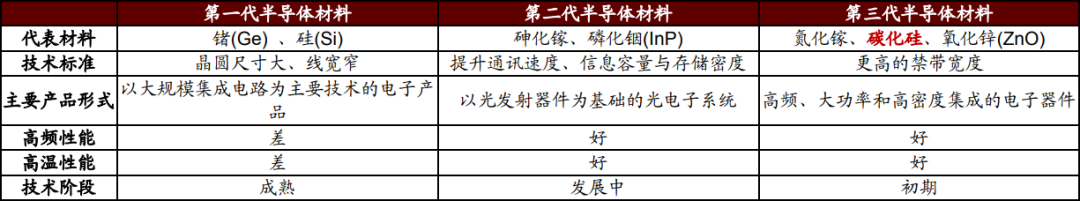
Data source: Material Person
The silicon carbide industry chain mainly includes the preparation of upstream silicon carbide substrate materials, the growth of epitaxial layers, midstream device manufacturing, and downstream application markets.
Silicon carbide industry chain
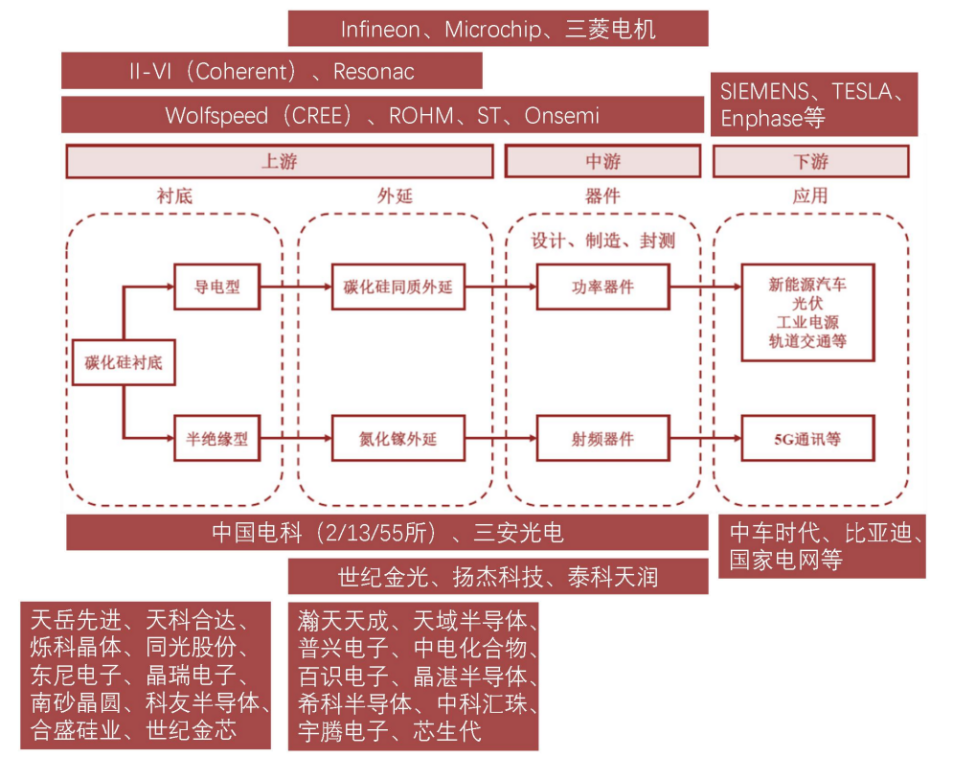
Data source: YOLE, Wide Bandgap Semiconductor Technology Innovation Alliance, Expert Commentary on Third Generation Semiconductors, Hantian Tiancheng Prospectus
From the cost structure perspective, the silicon carbide material segment accounts for 70% of the total value of the entire industry chain. The substrate is the segment with the highest technical barriers and the greatest value in the manufacturing process of silicon carbide power devices, accounting for about 47% of the total cost, with epitaxy accounting for about 23% and device manufacturing only accounting for 19%.
Cost composition of silicon carbide power devices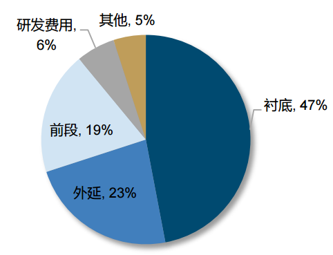
Data source: China Business Industry Research Institute
Silicon carbide substrates refer to single crystal materials formed from silicon carbide powder as the main raw material, through processes such as crystal growth, ingot processing, cutting, grinding, polishing, and cleaning. According to electrical performance, silicon carbide substrates can be divided into two categories: one type is semi-insulating silicon carbide substrates with high resistivity (resistivity ≥ 10^5Ω·cm), and the other type is conductive silicon carbide substrates with low resistivity (resistivity range of 15~30mΩ·cm). According to Yole data, in 2023, the global market size for conductive and semi-insulating silicon carbide substrates reached $684 million and $281 million, respectively.
Classification of silicon carbide substrates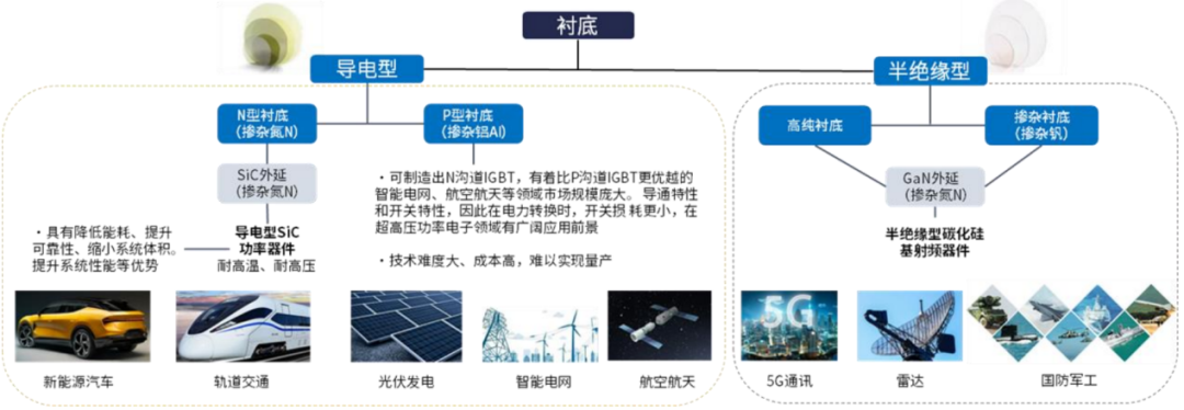 Data source: Yidu Data
Silicon carbide substrates are typically formed by chemical vapor deposition (CVD) to create an epitaxial layer on the wafer. On conductive substrates, silicon carbide epitaxial layers are grown to prepare silicon carbide homoepitaxial wafers, which are then used to manufacture silicon carbide power devices such as Schottky diodes, MOSFETs, and IGBTs. These devices have wide applications in downstream fields such as electric vehicle charging systems, photovoltaic inverter systems, rail transit traction systems, data center power management, smart grids, and aerospace.
On semi-insulating silicon carbide substrates, GaN heteroepitaxial layers are grown to produce GaN-on-silicon carbide epitaxial wafers, which can be used to make HEMTs and other microwave RF devices. These devices are mainly used in 5G communication base stations and terminal devices, intelligent interconnection systems for vehicle communication, radar and electronic countermeasure devices for defense applications, high-speed communication networks for data transmission, and electronic systems for aerospace vehicles.
2
Market is highly concentrated, supply side expands production and reduces costs
Compared to traditional silicon materials, the preparation efficiency of silicon carbide crystals is low, and there are high technical barriers in the growth of silicon carbide crystals and substrate processing. ① High temperature requirements: Compared to silicon-based substrates, silicon carbide substrates require very high temperatures (usually above 2000°C) during crystal growth, which cannot be monitored in real-time, making the process difficult; ② Slow crystal growth rate: In terms of crystal growth cycle, silicon carbide crystals take about a week to grow a 2cm ingot, while traditional silicon materials can grow nearly 2m long rods in just 2-3 days, resulting in low growth efficiency and limited production of silicon carbide substrates; ③ High crystal type requirements and difficulty in cutting and grinding: Silicon carbide crystals are prone to defects such as micropipes, polytype inclusions, and dislocations during the growth process. Silicon carbide single crystals include over 200 different crystal types, but only a few crystal structures (4H type) are required for the production of power devices. The growth process is prone to polytype inclusion defects due to crystal type transitions, so precise control of the silicon-carbon ratio, growth temperature gradient, crystal growth rate, and gas flow pressure is required. In terms of substrate processing, silicon carbide is a high brittleness material with hardness second only to diamond, making cutting time-consuming and prone to cracking.
Difficulties in silicon carbide substrate preparation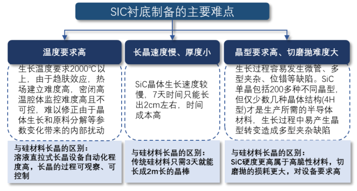
Data source: CSDN
The global silicon carbide substrate market shows a relatively concentrated competitive landscape, with leading companies dominating the market. According to a report by Fuji Economic, the American company Wolfspeed is the industry leader, holding the number one market share for several consecutive years, but is facing competitive pressure from other domestic substrate companies, with its share continuously declining to about 40% in 2024, down 5% from 2023. The American company Coherent (formerly II-VI) is also strong, having led in R&D and industrialization for many years, previously ranking second globally. Chinese companies are striving to catch up, with Tianyue Advanced and TankeBlue being industry leaders. In 2023, Tianyue Advanced surpassed Coherent (formerly II-VI) to become the second globally, with a market share of 22.8% in 2024. Another Chinese company, TankeBlue, ranks fourth in market share. Japan’s Rohm (which acquired Germany’s SiCrystal) also has strong competitiveness in the market through resource integration via mergers and acquisitions.
Global market share ranking of conductive silicon carbide substrates from 2019 to 2023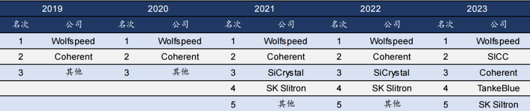
Data source: Fuji Economic
In 2024, the global silicon carbide industry will reach a turning point in supply and demand patterns, with rapid release of global 6-inch silicon carbide substrate capacity. The demand in the electric vehicle market is experiencing a phase of slowdown, leading to an oversupply in the 6-inch silicon carbide substrate market, with prices facing significant downward pressure in 2024. According to data from Jiemi Network, at the beginning of 2024, the price of leading silicon carbide substrate suppliers in China dropped by over 30%, with the price of 6-inch wafers falling below $500 in the third quarter. As price competition intensifies, some manufacturers are facing dual pressures of low capacity utilization and weak demand, while slow yield improvement and customer onboarding processes may accelerate the consolidation of the silicon carbide substrate industry.
In the future, the price of silicon carbide substrates will continue to decline, driven by two main factors: first, the reduction in unit costs brought about by the iteration and upgrading of production technologies and processes; as the yield in silicon carbide crystal growth and other processes improves and substrate sizes expand, the unit costs of various devices will continue to decrease. According to data from Wolfspeed, under the same chip size, the number of chips that can be cut from an 8-inch substrate is about 90% higher than that from a 6-inch substrate, while reducing edge waste by about 7%, resulting in a significant increase in productivity and efficiency. Secondly, the scale effect, as leading manufacturers of silicon carbide substrates, especially in China, expand their production capacity, they demonstrate significant scale effects in cost sharing, production automation, process optimization, supply chain procurement, and technology accumulation, thereby driving down substrate prices. The decline in substrate prices will promote the adoption of silicon carbide substrates in more downstream scenarios. Currently, 6-inch substrates are the mainstream product, with 8-inch substrates starting to be produced, and 12-inch substrates already having research and development samples.
Comparison of chip output quantities for 6-inch, 8-inch, and 12-inch silicon carbide substrates
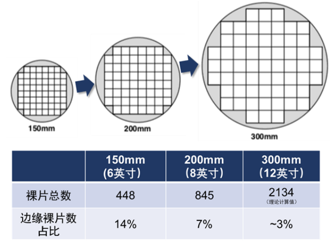
Data source: Tianyue Advanced Simple Fundraising Prospectus
Some international manufacturers have a first-mover advantage in the silicon carbide field and are moving quickly in the transition to 8-inch. Wolfspeed was the first in the world to launch 8-inch silicon carbide substrates in 2015, with actual mass production in 2022. Domestic companies have made breakthroughs in substrates, epitaxy, and devices, and are accelerating their catch-up to international leading levels. Tianyue Advanced, TankeBlue, Xilian Integrated, and Sanan Optoelectronics are all advancing their respective 8-inch silicon carbide substrate construction or expansion plans. In November 2024, Tianyue Advanced will be the first to release the world’s first 12-inch (300mm) N-type silicon carbide substrate product.
Progress of 8-inch silicon carbide substrate manufacturers
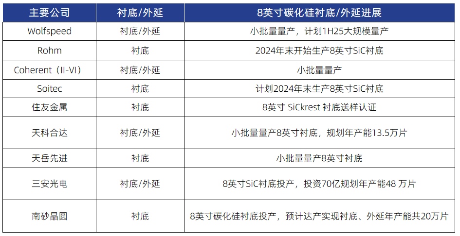
Data source: Jibang Compound Semiconductor, Semiconductor Industry Overview, eet-china
3
Downstream applications are thriving, driving demand growth
With the advantages of high frequency, low loss, high voltage resistance, and high temperature resistance of silicon carbide materials, silicon carbide power semiconductor devices can enhance the conversion efficiency of electricity in production and consumption processes, achieve smaller system sizes and higher power densities, and reduce the need for cooling systems, making them “energy efficiency multipliers” in fields such as electric vehicles, photovoltaic energy storage systems, power supply, and data centers.In electric vehicles, silicon carbide is mainly applied in key components such as motor drives, onboard chargers (OBC), and DC/DC converters. In motor drives, silicon carbide power modules replace traditional silicon-based IGBTs, reducing energy loss by 70% to 90%, increasing vehicle range by 10%, and supporting high power output in high-temperature environments. In OBCs, power modules convert external AC power to DC power for battery charging, with silicon carbide power modules reducing charging losses by 40%, achieving faster charging speeds and enhancing user experience. In DC/DC converters, their role is to convert the high-voltage battery’s DC power to low-voltage DC power for onboard devices, with silicon carbide power modules improving efficiency by reducing heat generation and energy loss by 80% to 90%, minimizing the impact on vehicle range.In photovoltaic energy storage, silicon carbide power semiconductor devices can be used in inverters, boost converters, and energy storage converters in photovoltaic components and energy storage systems. These devices enhance the performance of photovoltaic systems by improving energy conversion efficiency, reducing losses, and minimizing the size and weight of components, thereby broadening their application range. Compared to traditional silicon-based devices, silicon carbide-based photovoltaic inverters can improve conversion efficiency by 1% to 3%, with size and weight typically reduced by 40% to 60%.In 5G communication base stations, semi-insulating silicon carbide-based GaN RF devices can achieve higher signal transmission frequencies and power, improving communication quality and coverage. In power grid applications, the use of silicon carbide power semiconductor devices can significantly reduce the number of devices required, equipment size and weight, energy losses, and system complexity, while also reducing the need for cooling equipment, lowering the overall construction costs of power systems.Emerging application scenarios are opening up new growth spaces. In the AI data center field, data centers account for about 3% of global electricity consumption, and silicon carbide power modules are 5% more efficient than traditional silicon devices. If 30% of global data centers adopt silicon carbide technology, it could save over $20 billion in electricity costs annually. Currently, the United States has begun large-scale deployment of silicon carbide modules, while domestic companies are accelerating to catch up with this trend. In the AR glasses field, a pair of AR glasses requires two 4-inch silicon carbide substrates. If the annual sales of AR devices reach 1 billion units (comparable to the smartphone market size), the demand for silicon carbide will be ten times that of the electric vehicle sector. Currently, companies like Huawei and Xiaomi have already initiated related R&D work.Global market size of silicon carbide power semiconductor devices (by application field), measured by sales revenue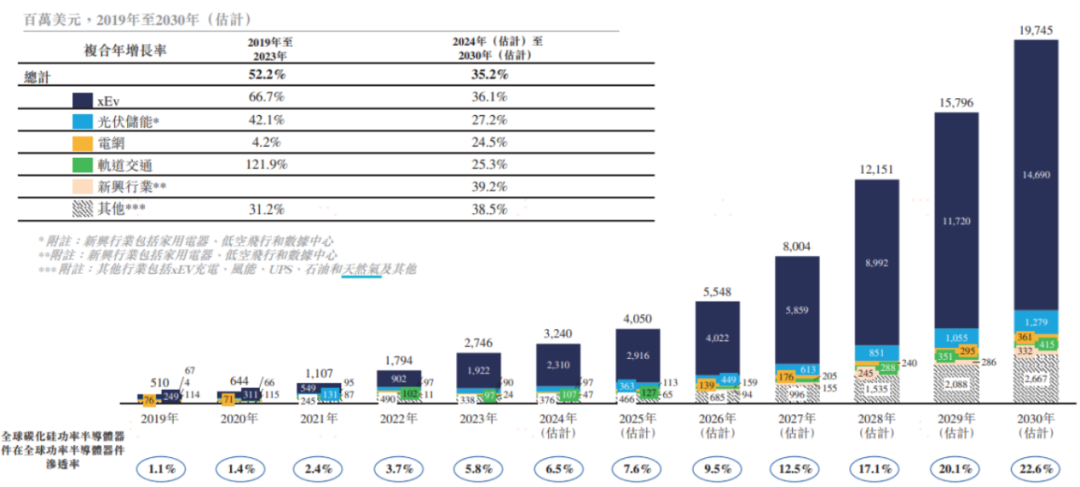
Data source: Yole, Frost & Sullivan
According to Frost & Sullivan data, from 2019 to 2023, the global silicon carbide power semiconductor device industry market size has significantly increased from $510 million to $2.7 billion, with a compound annual growth rate of 52.2%. It is expected that by 2030, the market size will reach approximately $19.7 billion; the penetration rate of global silicon carbide power semiconductor devices in the global power semiconductor device market has increased from 1.1% to 5.8%, and is expected to reach 22.6% by 2030. This growth trend not only reflects the strong demand for silicon carbide power semiconductor devices but also directly drives the growth in demand for silicon carbide substrates. With the widespread application of silicon carbide power semiconductor devices in strategic emerging industries such as electric vehicles, photovoltaic wind energy, and 5G communication, substrates, as key materials for producing silicon carbide devices, will see explosive growth in market demand. The global silicon carbide substrate market size has grown from 2.6 billion RMB in 2019 to 7.4 billion RMB in 2023, with a compound annual growth rate of 29.4%. It is expected that by 2030, the market size will reach 66.4 billion RMB, with a compound annual growth rate of 39.0%.
From specific application fields, from 2019 to 2023, the compound annual growth rate of global revenue from silicon carbide power semiconductor devices used in electric vehicles (xEV) reached 66.7%, while from 2024 to 2030, the compound annual growth rate in the xEV field will still be as high as 36.1%, continuing to lead the global silicon carbide power semiconductor device market growth. Photovoltaic energy storage, power grids, and rail transit fields also show strong growth momentum, with projected compound annual growth rates of 27.2%, 24.5%, and 25.3%, respectively, during the forecast period. Emerging application fields such as household appliances, low-altitude flight, and data centers will exhibit the fastest growth rates, with projected compound annual growth rates of global revenue from silicon carbide power semiconductor devices in these fields expected to reach 39.2%.