Content Summary1. Computational Demands of Large Models: The need for massive parameter storage, dense matrix operations, and frequent memory access drives chip architecture towards high performance and low latency;2. Challenges in Chip Design: The imbalance between chip computing power and bandwidth, with the “memory wall” becoming the biggest bottleneck to development;3. Innovative Chip Architecture Design: Addressing the “memory wall” challenge, dedicated chips focus on improving energy efficiency, aiming to enhance on-chip bandwidth and even break through the traditional “Von Neumann” architecture;4. Co-design of Software and Hardware as a New Growth Point: From algorithm design to hardware optimization, the deep integration of software and hardware is essential for achieving high performance and energy efficiency in the era of large models;5. Ecological Construction of Domestic Chips: Achieving efficient migration of software ecosystems, addressing gaps in cluster communication technology, and building a self-controllable technological system.(The full text is approximately 4600 words, with a reading time of about 12 minutes)
The following content is organized from the “He Shanzhi Stone Can Attack Jade” interdisciplinary salon held on November 23, 2024, at the University of Chinese Academy of Sciences, presented by Dr. Ze Rui Fang from the School of Frontier Interdisciplinary Sciences.
01What Requirements Do Large Models Place on Chip Architecture?The computational demands of the large model era are fundamentally reshaping the design concepts of chips and systems. Traditional chip design primarily optimizes for general computing or graphics rendering, while large model computations exhibit distinctly different characteristics: massive parameter storage, dense matrix operations, and frequent memory access, which pose significant challenges to existing architectures in terms of efficiency and performance. The computation process of large language models is divided into two phases: the Prompt phase (Prefill) and the Token generation phase (Decode), where the former processes user input and the latter generates output content one token at a time. In this process, General Matrix Multiply (GEMM) and General Matrix-Vector Multiply (GEMV) are key computational operations that place extremely high demands on chip computing capabilities.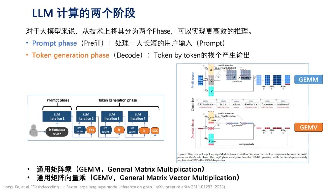
“The memory wall” has become the biggest bottleneck restricting the development of large models. Over the past 20 years, the floating-point computing power of computing chips has increased by 60,000 times, while memory bandwidth has only increased by 100 times. This gap leads to situations where, even with top-tier computing units, chips often remain in a “starved” state during large model training and inference—significant computing resources are forced to wait for data and cannot operate efficiently.
02Innovative Chip Architecture Paths to Break Through the “Memory Wall”In response to the “memory wall” challenge, the chip design field is exploring multiple hardware innovation paths. The new generation of GPUs represented by Nvidia optimizes data flow through dedicated AI computing acceleration engines and significantly increased on-chip cache and bandwidth; TPU chips represented by Google and Cambricon achieve higher energy efficiency computing models through circuit designs tailored for specific AI algorithms; additionally, the compute-in-memory architecture, as a typical representative of non-Von Neumann architectures, fundamentally eliminates data transfer bottlenecks by integrating computing units directly into memory arrays.General-purpose Graphics Processing Units (GPGPUs) are currently the main chip type for large model computations. Their core concepts include storage locality, increased parallelism, and enhanced asynchronicity. By ensuring that data is stored close to the storage units, data transfer times can be fundamentally reduced. According to Little’s Law, when memory access time is fixed, the best approach is to increase parallelism to mask latency, such as processing large batches of data samples simultaneously in deep learning. Finally, various asynchronous memory access microarchitectures can pre-fetch the data needed for computation to reduce waiting times for data during computation.Nvidia’s GPUs are also equipped with Tensor Cores and a Transformer Engine specifically designed to accelerate GEMM operations and Transformer layer computations, significantly enhancing the efficiency of large model computations. At the software level, deep collaboration with deep learning libraries such as CUDA and cuDNN optimizes algorithm implementations, further improving computational performance.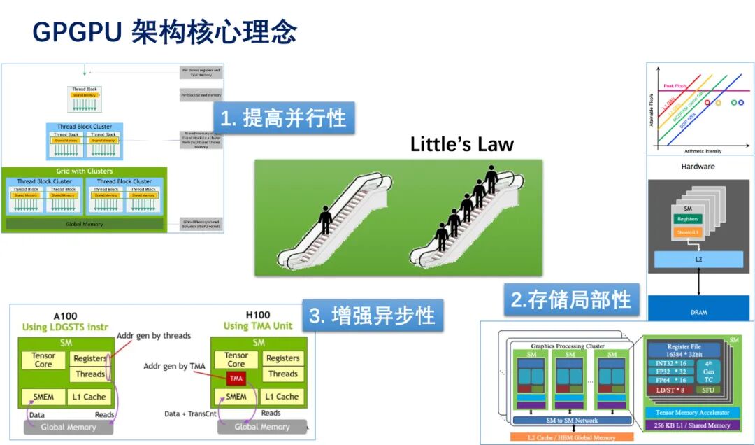 In response to the dense matrix computation demands posed by large models, Tensor Processing Units (TPUs) specifically designed to accelerate such computations can achieve higher energy efficiency. TPUs significantly enhance computational efficiency through hardware optimizations for matrix multiplication and vector operations. Their pulse array architecture reduces data movement overhead through stream processing, demonstrating outstanding performance and energy consumption advantages during the training and inference of large models, reflecting the immense potential of dedicated hardware in specific computational scenarios. Today, TPUs are widely used in data centers, edge, and mobile devices, providing robust support for large model training and inference. In comparison, GPGPUs are based on Single Instruction Multiple Threads (SIMT) architecture, offering programming flexibility but facing branching issues, compiler and architecture complexity, and higher power consumption; TPUs are based on Single Instruction Multiple Data (SIMD) architecture, with a simpler hardware architecture. Both have advantages in different application scenarios, with GPGPUs suitable for general computing and scenarios requiring high flexibility, while TPUs focus more on specific large-scale matrix computation tasks.Enhancing on-chip bandwidth has become a key direction for breaking through the “memory wall” challenge and unlocking chip performance potential. Insufficient on-chip bandwidth not only leads to idle computing cores waiting for data but also exacerbates chip energy consumption, severely limiting overall performance. Wafer Scale chips represent another innovative approach compared to GPUs and TPUs, focusing on treating the entire wafer as a single chip, thereby reducing inter-chip interconnection losses and achieving ultra-large-scale on-chip bandwidth. This technology constructs a complete computing system at the wafer level, eliminating connection components such as pins and substrates in traditional chip packaging, allowing data to be transmitted rapidly within the wafer-level range. For example, the WSE-3 chip launched by Cerebras Systems, manufactured using a 5-nanometer process, integrates up to 40 trillion transistors on a chip with a side length of 21.5 cm and an area of 46,225 square millimeters, featuring 900,000 AI-optimized computing cores and providing 125 FP16 PFLOPS. This colossal chip occupies nearly the entire 300 mm silicon wafer, with an area 57 times larger than Nvidia’s H100 GPU, a 52-fold increase in core count, an 800-fold increase in chip memory, and a staggering 7,000-fold increase in memory bandwidth, with structural bandwidth increasing by over 3,700 times.The traditional “Von Neumann” architecture exacerbates the “memory wall” problem, severely limiting computational efficiency. The physical separation of memory and computing units necessitates frequent data transfers between the two, leading to significant data transfer overhead and creating the “Von Neumann bottleneck”—computing units remain idle while waiting for data, severely restricting computational efficiency. To address this bottleneck, Computing-in-Memory technology has emerged, which embeds computing functions directly into memory, reducing data transfer overhead. Specifically, during matrix-vector multiplication, matrix data is stored in the memory array of the compute-in-memory chip, while vector data is input in the form of voltage or current, allowing for parallel computation through the resistive characteristics of storage units, directly outputting computation results and avoiding the extensive data transfer process between storage and computing units. In large model inference, as the number of tokens increases, the time spent on GEMV and memory access copies becomes significant, leading to low GPU resource utilization. Integrating GEMV into the compute-in-memory chip can significantly enhance GPU utilization and energy efficiency, reduce data transfer overhead, and improve computational efficiency, providing a new breakthrough direction for large model computations.
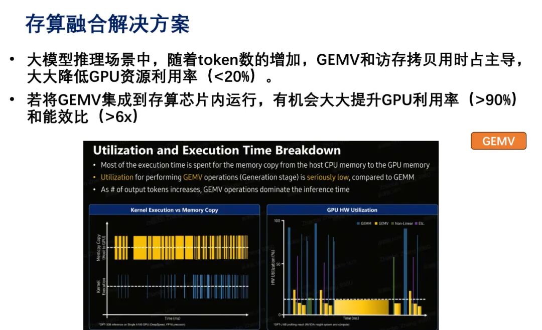 In today’s diverse AI model structures, it is even more important to conduct comprehensive chip performance evaluations based on task requirements. The Roofline Model is an important tool for assessing chip performance, determined by the computational power and bandwidth limits of the computing platform. Computational power determines the height of the “roof,” while bandwidth determines the slope of the “eaves.” When the model’s computational intensity is low and bandwidth-limited, performance depends on bandwidth and computational intensity; when computational intensity is high and reaches the computational power limit, performance is constrained by computational power. For example, in the case of the VGG16 and MobileNet V1 models, although the lightweight MobileNet has a computational load that is 1/30 of VGG, it is limited by bandwidth, achieving a performance P that is only 1/3 of VGG, theoretically resulting in a running speed only 10 times that of VGG.
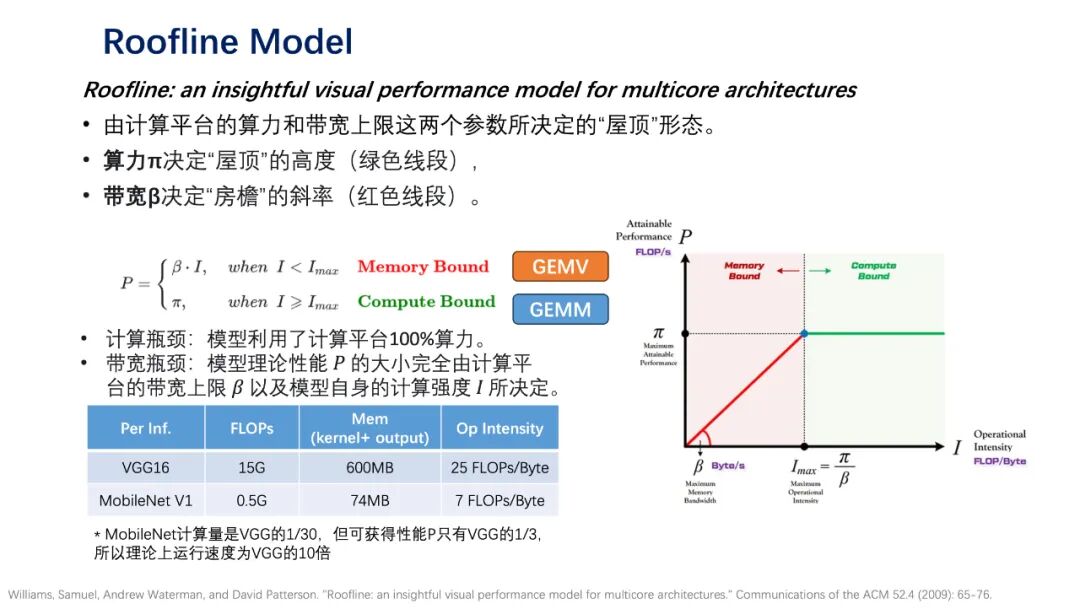 03The New Journey of Software and Hardware Co-developmentRelying solely on hardware innovation is insufficient to completely address the challenges; co-design of software and hardware has become the only path in the era of large models. This collaboration not only refers to developing optimization libraries for specific hardware but also considers hardware characteristics from the model algorithm design stage, such as neural network architecture search, mixed precision training, and quantization-aware training techniques. Nvidia’s dominance in the AI chip market stems from establishing a complete software-hardware co-development ecosystem from CUDA, cuDNN to TensorRT, achieving optimal matching between algorithms and hardware. At the GTC 2025 conference, Nvidia CEO Jensen Huang emphasized that the primary performance leap for Nvidia’s GPUs comes from the company’s own architectural innovations and breakthroughs at the software level.The large model inference framework plays a bridging role in software-hardware collaboration. Different chip architectures possess unique computational characteristics and storage structures, and inference frameworks must be customized to adapt to chip hardware characteristics to fully leverage chip performance.The successful practice of DeepSeek demonstrates that software-hardware collaboration is the only path for AI chips to achieve high performance, high energy efficiency, and flexible adaptability.To achieve domestic substitution, efficiently migrating existing software foundations to domestic architectures is a key aspect. The traditional software ecosystem has long relied on foreign technology systems; building a software system compatible with domestic chips from scratch not only requires massive human and time investments but also risks technological discontinuity and ecological fragmentation. Smooth migration of software can retain the functionality and value of existing software while accelerating the maturity of the domestic software-hardware system, forming a virtuous development cycle. In terms of portability, the MUSA architecture and software stack from Moore Threads demonstrate excellent compatibility with CUDA, achieving efficient operation across different hardware platforms by replacing corresponding acceleration libraries. OpenAI Triton also provides a feasible path for running large models on various custom accelerators, reducing development costs and improving development efficiency.Large models are highly dependent on cluster communication technology, and domestic solutions lag behind international advanced levels. Cluster communication capability is central to the collaborative operation of multiple chips; currently, domestic cluster communication solutions fall short in key indicators such as bandwidth and latency compared to international advanced levels. The large-scale parameter updates and distributed computing tasks required for large model training necessitate data exchange through cluster communication; if communication efficiency is insufficient, even if individual chip performance is outstanding, overall computational efficiency will significantly decline due to data transfer bottlenecks.
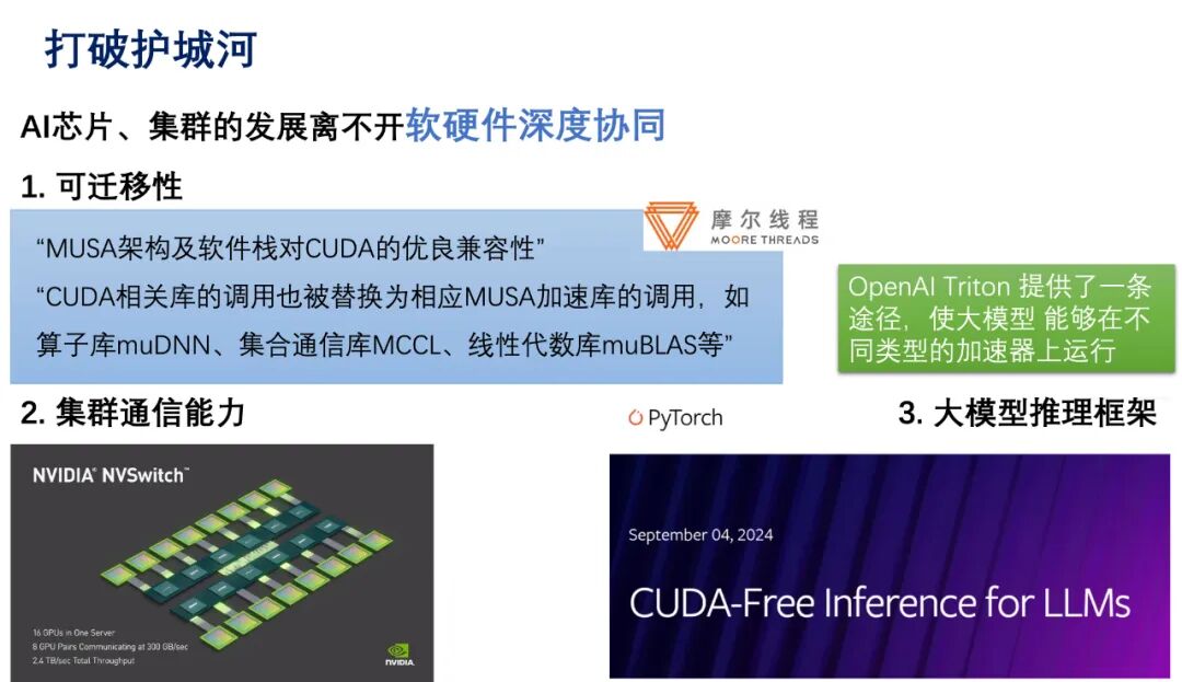
The revolution in chip and system architecture is not only a technological evolution but also concerns national AI competitiveness and digital sovereignty. In an era where large models have become a key strategic resource, mastering the autonomy of core chip and system technologies far exceeds mere commercial significance, becoming an important guarantee for the security of national digital infrastructure. With changes in the international landscape, the autonomy and controllability of technology have increasingly become a key part of national strategy; without compatible software, domestically developed hardware is like “cooking without rice”; and advanced software cannot exert its effectiveness without suitable hardware. Only through deep integration and collaborative innovation of software and hardware can a self-controllable technological system be constructed, breaking foreign technological monopolies and achieving self-reliance and strength in the field of technology.
References
[1] Hong, Ke, et al. “Flashdecoding++: Faster large language model inference on GPUs.” arXiv preprint arXiv:2311.01282 (2023).
[2] Rui Xu, Sheng Ma, Yang Guo, and Dongsheng Li. 2023. A Survey of Design and Optimization for Systolic Array-based DNN Accelerators. ACM Comput. Surv. 56, 1, Article 20 (January 2024), 37 pages.
[3] Fujiki, Daichi, et al. In-/near-memory Computing. Morgan & Claypool Publishers, 2021.
[4] Williams, Samuel, Andrew Waterman, and David Patterson. “Roofline: an insightful visual performance model for multicore architectures.” Communications of the ACM 52.4 (2009): 65-76.
[5] C++ Programming Guide: https://docs.nvidia.com/cuda/cuda-c-programming-guide/index.htmlCUDA.
[6] Samsung Processing in Memory Technology at Hot Chips 2023: https://www.servethehome.com/samsung-processing-in-memory-technology-at-hot-chips-2023/.
Coordinated by: He Shan Publicity Department
Content: Ze Rui Fang
Reviewed by: Bo Yuan Zheng
Typeset by: Ying Wang


TA SHANThe He Shan Interdisciplinary Innovation Association at the University of Chinese Academy of Sciences aims to “break down disciplinary barriers and expand cognitive boundaries,” dedicated to building a platform for university students to engage in interdisciplinary communication, empowering the growth of future leading technology talents, and promoting the interdisciplinary integration and development for the implementation of the strategy of strengthening the country through science and education, talent-driven development strategy, and innovation-driven development strategy.Long press the QR code belowto follow the “He Shan Interdisciplinary” public account▼