
Click
Blue Text
Follow Us~
1
Cutting (CUT)
Cutting is the process of cutting the raw copper-clad board into pieces that can be made into boards on the production line. First, let’s understand a few concepts with the EDA365 Electronics Forum:
(1) UNIT: A UNIT refers to the unit graphic designed by the PCB design engineer.
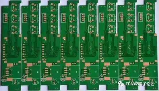
(2) SET: A SET refers to a whole graphic formed by combining multiple UNITS for reasons such as improving production efficiency and convenience. This is what we commonly call a panel, which includes unit graphics, process edges, etc.
(3) PANEL: A PANEL refers to a board formed by combining multiple SETS along with tool board edges during the production process to improve efficiency and convenience.
2
Inner Dry Film (INNER DRY FILM)
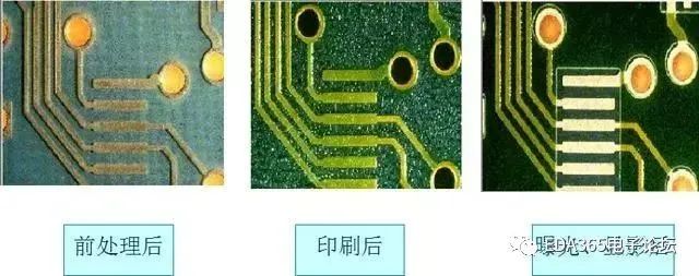
The inner dry film is the process of transferring the inner circuit graphics onto the PCB board.
In PCB manufacturing, we often mention the concept of graphic transfer, as the creation of conductive graphics is fundamental to PCB production. Therefore, the graphic transfer process is of great significance to PCB manufacturing.
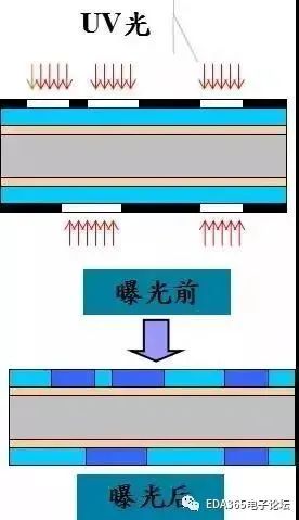
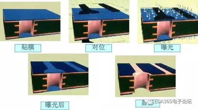
The inner dry film includes multiple processes such as inner film attachment, exposure development, and inner etching.
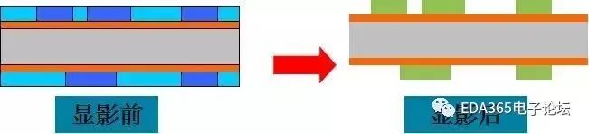
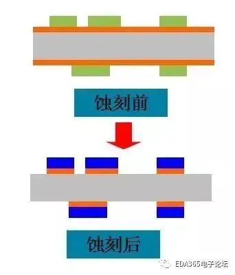
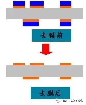
The inner film attachment involves attaching a special photosensitive film to the surface of the copper board, which is what we call dry film. This film solidifies upon exposure to light, forming a protective film on the board. Exposure development involves exposing the board with the attached film; the parts that are exposed to light are solidified, while the parts that are not remain as dry film. After development, the non-solidified dry film is removed, and the board with the solidified protective film is etched. After the film stripping process, the inner circuit graphics are transferred onto the board.
The entire process flow is shown in the image below.
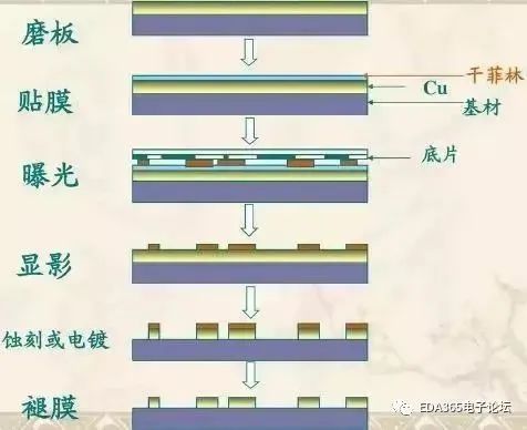
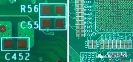
For designers, the main considerations are the minimum line width, spacing control, and uniformity of wiring.
Too small spacing can cause film trapping, leading to unremovable film and short circuits. If the line width is too small, the adhesion of the film will be insufficient, causing open circuits. Therefore, the safe spacing during circuit design (including line-to-line, line-to-pad, pad-to-pad, line-to-copper surface, etc.) must consider the safety spacing during production.
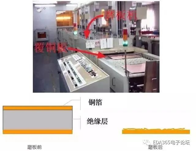
(1) Pre-treatment: Board Grinding
The main function of board grinding is to address the issues of surface cleanliness and roughness. It removes oxidation and increases the roughness of the copper surface to facilitate the attachment of the film to the copper surface.
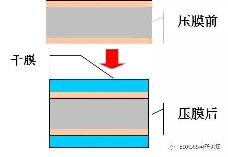
(2) Film Attachment
The treated substrate is attached with dry film or wet film through hot pressing or coating, facilitating subsequent exposure production.
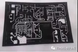
(3) Exposure
The film is aligned with the substrate with the attached dry film, and ultraviolet light is used in the exposure machine to transfer the film graphics onto the photosensitive dry film.
Physical image of the film.
(4) Development
Using a developer solution (sodium carbonate) with weak alkalinity to dissolve and wash away the unexposed dry film/wet film, leaving the exposed parts intact.
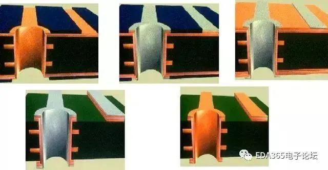
(5) Etching
After the unexposed dry film/wet film is removed by the developer, the exposed copper surface is revealed, which is then dissolved and etched away using acidic copper chloride to obtain the desired circuit.
(6) Film Stripping
The exposed dry film protecting the copper surface is stripped off using sodium hydroxide solution, revealing the circuit graphics.
3
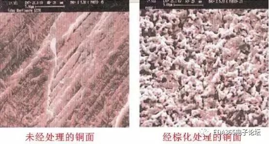
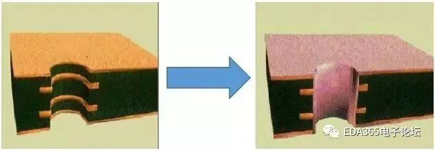
Brown Oxidation
Purpose: To form micro-roughness and an organic metal layer on the inner copper surface, enhancing the bonding strength between layers.
Process Principle: A uniform organic metal layer structure with good bonding characteristics is produced through chemical treatment, controlling the roughness of the inner copper layer surface before bonding with the prepreg, thereby enhancing the bonding strength after pressing.
4
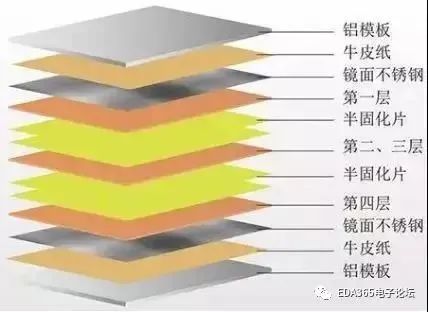
Lamination
Lamination is the process of bonding various layers of circuits into a whole using the adhesive properties of prepreg. This bonding is achieved through the mutual diffusion and penetration of large molecules at the interface, resulting in interweaving, thus pressing the discrete multilayer boards with prepreg into the required layers and thickness of multilayer boards.
In actual operation, materials such as copper foil, bonding sheets (prepreg), inner boards, stainless steel, isolation boards, kraft paper, and outer steel plates are stacked according to process requirements.
For designers, the first consideration in lamination is symmetry. According to the EDA365 Electronics Forum, during the lamination process, the board will be affected by pressure and temperature, and there will still be stress in the board after lamination. Therefore, if the laminated board is not uniform on both sides, the stress on the two sides will be different, causing the board to bend to one side, greatly affecting the PCB performance.
Moreover, even on the same plane, if the copper distribution is uneven, it will cause different resin flow rates at each point, resulting in slightly thinner areas where copper is less and slightly thicker areas where copper is more.
To avoid these problems, the EDA365 Electronics Forum reminds everyone that during design, factors such as the uniformity of copper distribution, symmetry of stacking, design layout of blind and buried holes, etc., must be considered in detail.
5
Drilling
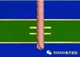
To create vias between layers of the circuit board for inter-layer connectivity.
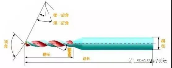
The legendary drill bit.
6
Copper Plating
(1) Electroless Copper Plating
Also known as chemical copper, the PCB board after drilling undergoes a redox reaction in the electroless copper tank, forming a copper layer to metallize the holes, allowing the previously insulated substrate surface to deposit copper, achieving electrical connectivity between layers.
(2) Board Plating
This process thickens the copper on the surface and inside the holes of the freshly electroless copper PCB board to 5-8um, preventing oxidation and micro-etching of the thin copper inside the holes before graphic electroplating.
7
Outer Dry Film
The process is the same as that of the inner dry film.
8
Outer Graphic Electroplating, SES
The copper layers of the holes and circuits are electroplated to a certain thickness (20-25um) to meet the final PCB copper thickness requirements.
Excess copper on the board surface is etched away, revealing the useful circuit graphics.
9
Solder Mask
Solder mask, also known as anti-solder or green oil, is one of the most critical processes in PCB manufacturing. It primarily involves applying a layer of solder mask through screen printing or coating on the board surface, followed by exposure and development, exposing the pads and holes to be soldered while covering other areas with solder mask to prevent short circuits during soldering.
10
Silkscreen Characters
The required text, logo, or component symbols are printed on the board surface using a stencil printing method, then exposed to ultraviolet light.
11
Surface Treatment
The solderability of bare copper is excellent, but it is prone to moisture and oxidation when exposed to air for long periods, tending to exist in the form of oxides rather than maintaining its original copper state. Therefore, surface treatment of the copper surface is necessary. The primary purpose of surface treatment is to ensure good solderability or electrical performance.
Common surface treatments include: tin spraying, gold immersion, OSP, tin immersion, silver immersion, nickel-palladium gold, electroless gold, and gold fingers.
12
Forming
The PCB is cut to the required external dimensions using a CNC forming machine.
13
Electrical Testing
The board’s state is simulated, and electrical performance is checked to see if there are any opens or shorts.
14
Final Inspection, Sampling, Packaging
The board’s appearance, dimensions, hole diameter, board thickness, markings, etc., are checked to meet customer requirements. Qualified products are packaged into bundles for easy storage and transportation.

Meizhou City Printed Circuit Industry Association
Source: PCB Media
Copyright Statement: The copyright of the above text and images belongs to the original author. The “Meizhou City Printed Circuit Industry Association” is sharing this as a reprint. If there are any copyright issues, please contact us for deletion.