Introduction
Recently, I have come across some new processes, and during meetings with foundries, the HCI mechanism is frequently mentioned. What is the HCI mechanism? In the wave of miniaturization of modern electronic devices, the size of transistors on chips has shrunk to the nanometer scale. While we enjoy faster and more integrated electronic products, a “silent battle” concerning device lifespan is taking place in the microscopic world of semiconductor physics. Among these, Hot Carrier Injection (HCI) is one of the main reliability threats. Understanding HCI is not only a compulsory course for chip designers but also a window into the physical mysteries of the microscopic world.
1
What are Hot Carriers?

To understand HCI, we first need to grasp the meaning of “hot carriers”.
In semiconductors, “carriers” refer to free electrons or holes that carry current. At room temperature, they undergo random thermal motion, with their average kinetic energy related to temperature. However, when we apply voltage to a transistor (taking NMOS as an example), the electrons in the channel are accelerated by the lateral electric field between the source and drain, gaining average kinetic energy far exceeding their thermal equilibrium state.
These electrons with ultra-high kinetic energy are referred to as “hot carriers”. Here, “hot” does not refer to high temperature but describes their energy state being extremely high, akin to a baseball thrown with great force, moving much faster than the thermal motion of air molecules.
2
The HCI Mechanism

The entire process of HCI can be vividly understood as a microscopic “car accident” triggered by high-speed particles. Taking NMOS transistors as an example, we analyze it step by step:

Step 1: Acceleration – Carriers Gain Energy
When the MOSFET operates, the electric field strength reaches its maximum in the region of the channel near the drain (because the potential difference is most intense here). Electrons flow from the source to the drain, and as they pass through this high electric field region, they are sharply accelerated, much like a race car flooring the accelerator on the final straight.

Step 2: Collision – Energy Transforms into Destructive Potential
These accelerated hot electrons have two main fates:
Collision Ionization: High-energy electrons collide with silicon lattice atoms, knocking electrons from the valence band and generating new electron-hole pairs. The newly generated electrons may also be accelerated, continuing to trigger more collisions, forming what is known as the “avalanche effect”. This process generates additional leakage current (substrate current).
Gaining Sufficient Kinetic Energy: Some electrons are fortunate enough not to undergo significant collisions but gain kinetic energy through electric field acceleration, exceeding the barrier height between silicon and the gate oxide layer (approximately 3.1 eV for electrons).
Step 3: Injection – Breaking into the “Forbidden Zone”
Those hot electrons with kinetic energy exceeding the barrier height gain the ability to “jump the wall”. They overcome the barrier and inject into the gate oxide layer, which should be an insulator. This marks the beginning of the entire destructive process.
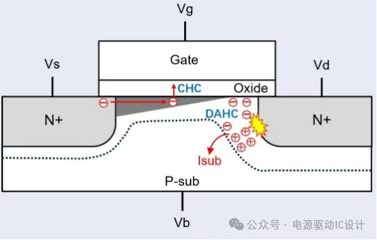
(Image source: Internet, please delete if infringing)
3
Effects and Consequences of HCI

The degradation of devices caused by the HCI effect is cumulative and permanent. Its direct impacts include:
01
Device Level
Vth drift, gm decrease, leading to slower switching speeds.
02
Circuit Level
For digital circuits, it can cause timing disruptions (setup/hold time violations) and logical errors; for analog circuits, it can worsen gain, matching accuracy, and noise performance.
03
System Level
Ultimately leading to substandard chip performance, shortening the lifespan of the entire electronic product.
4
How to Quantify and Combat HCI?

In chip design, engineers must conduct strict assessments and preventive measures against HCI.

Quantification Model:
The lifespan of HCI is typically predicted using a lifetime model, a classic form of which is:

Where τ is the time to reach a specific degradation standard (e.g., Vth offset of 10mV), Id is the leakage current, W is the channel width, Φ is the barrier height, and E is the electric field. By conducting accelerated lifetime testing (under high temperature and high voltage), model parameters can be fitted to predict device lifespan under normal usage conditions.

Countermeasures
-
Circuit Design
Lower Operating Voltage: This is the most effective method, as the electric field strength is directly related to voltage.
Avoid Overdriving: Carefully design signal swing to prevent transistors from operating under high electric field stress for extended periods.
-
Device/Process Optimization
Lightly Doped Drain (LDD) Structure: This is the most classic process invention to combat HCI. Inserting a lightly doped region between the channel and heavily doped drain region can effectively disperse and reduce the maximum electric field strength, thereby reducing the generation of hot electrons at the source.
Strained Silicon Technology: By enhancing carrier mobility, the same drive current can be obtained at lower voltages, indirectly alleviating HCI.
High-k Metal Gate: Using high-k dielectrics (such as HfO₂) instead of traditional SiO₂ can achieve the same equivalent oxide thickness (EOT) at a larger physical thickness, thereby reducing gate direct tunneling current and enhancing control over the channel electric field.
New Device Structures: Three-dimensional structures like FinFETs have better gate control capabilities and more uniform channel electric field distribution, helping to suppress HCI.
Conclusion and Outlook
Hot Carrier Injection (HCI) is a fundamental reliability issue that arises with the miniaturization of MOSFETs. It profoundly reveals the close relationship between macro circuit performance and micro physical phenomena. From the initial acceleration, collision, to the final injection and entrapment, the HCI mechanism fully depicts the progressive and irreversible damage caused by high-energy particles to insulating media.
As semiconductor technology nodes continue to advance towards 3nm, 2nm, and even smaller, the gate oxide thickness has thinned to just a few atomic layers, and the reduction of operating voltage is approaching its limits. In this context, the challenges of HCI have not disappeared but have emerged in more complex forms (e.g., coupling effects with BTI). A deep understanding of the HCI mechanism and continuous innovation remain key to advancing semiconductor technology, ensuring that every chip in our hands can operate at high speed while maintaining a long and reliable lifespan.

END