
NVIDIA released the new generation centralized vehicle computing platform, NVIDIA DRIVE Thor, on September 20, capable of running advanced driver assistance applications and in-vehicle infotainment applications on a single secure and reliable system. It provides 20 trillion floating-point operations performance (20 trillion 8-bit floating-point operations). NVIDIA’s contemporary product is Orin, with a computing power of 256 TOPS. Following that is the released Altan, with a computing power of 1000 TFLOPS. The computing power of this Thor, at 2000 TOPS, is indeed shocking (however, the chip won’t be available until 2025, so it seems like a bit of a distant PPT product).
This raises a question: what kind of computing power is this? How is it calculated/standardized?
First, let’s look at the explanations of three terms:
TFLOPS (teraFLOPS) equals one trillion (10^12) floating-point operations per second. FLOPS (Floating-point operations per second) refers to the number of floating-point operations per second. TOPS (Tera Operations Per Second) means 1 TOPS represents one trillion (10^12) operations that the processor can perform per second. DMIPS: Dhrystone Million Instructions executed Per Second, which counts the number of million instructions executed in one second, indicating the processing capability of the system in that second.
Given that NVIDIA’s Thor is still a PPT and there are no concrete product details yet, let’s first look at the computing power of existing chips, specifically Tesla’s FSD (the chip for autonomous driving, different from the intelligent cockpit SOC).
===============================================
NPU Computing Power
NPU Computing Power. TOPS only refers to the trillion operations per second of the processor, and it needs to be combined with specific data type precision to convert to FLOPS. The number of MAC (Multiply Accumulate) operations at 8-bit precision is halved compared to that at FP16 (half-precision/16-bit floating-point). Note: NVIDIA, Intel, and Arm have collaborated to write the white paper on FP8 Formats for Deep Learning. Currently, the industry has transitioned from 32 bits to 16 bits, and now even to 8 bits (FP8 precision: 8-bit floating-point operation specification), which is also why NVIDIA uses FP8 to represent computing power. The 2000 TOPS mentioned above for Thor is referring to this.
In NPU, chips use MAC arrays (Multiply Accumulate) to accelerate neural networks, as many operations (such as convolution operations, dot product operations, matrix operations, digital filter operations, and even polynomial evaluation operations) can be decomposed into several MAC instructions, thus improving the efficiency of these operations. MAC matrices are core to AI chips and represent a mature architecture. NVIDIA also uses 3D cube computing units in examples to complete matrix multiplication and accumulation operations. TOPS is the number of operations performed by MAC in one second, calculated as:
TOPS = MAC matrix rows * MAC matrix columns * 2 * clock frequency;
Note: The 2 in the formula can be understood as one MACC (multiply-accumulate operation) consisting of one multiplication and one addition, thus accounting for two operation actions. Let’s take Tesla’s autonomous driving FSD chip as an example.
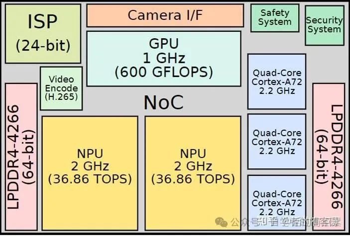
According to Tesla’s information, the target for this chip is Level 4 and Level 5 autonomy. The FSD chip is manufactured using Samsung’s 14nm process technology at their Austin, Texas plant, integrating three quad-core Cortex-A72 clusters, totaling 12 CPUs, with a working frequency of 2.2GHz, one (ARM’s) Mali G71 MP12 GPU, and two NPUs with a working frequency of 2GHz, along with various other hardware accelerators. The FSD chip supports up to 128-bit LPDDR4-4266 memory.
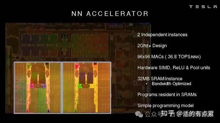
The right side of the image clearly describes: “ 96*96 MACs (single core) (36.8 TOPS/NNA)”, based on the calculation formula above:
TOPS = MAC matrix rows * MAC matrix columns * 2 * clock frequency = 96 * 96 * 2 * 2G = 36.864 TOPS (single core)
The above result matches the computing power number in the image, representing the NPU single-core computing power. The Tesla FSD (Full Self-Driving) IC contains two NPUs: each cycle reads 256 bytes of activation data and another 128 bytes of weight data from SRAM into the MAC array. Each NPU has 96×96 MACs, and regarding precision, multiplication is 8×8 bits, and addition is 32 bits, with the choice of these two data types largely depending on their efforts to reduce power consumption (for example, a 32-bit FP adder consumes about nine times more power than a 32-bit integer adder). As shown in the image, at a working frequency of 2GHz, the computing power of each NPU is 36.86 TOPS, and the peak computing power of the FSD chip is 73.7 TOPS (the sum of the computing power of two single-core NPUs).
=====================================================
CPU Computing Power (ARM Core)
Quectel launched the SIP module AG855G based on the SA8155P platform, which is described on their official website as having an AI integrated computing power of 8 TOPS. What about CPU computing power?
Qualcomm’s official website and product summary do not provide direct numerical descriptions of the CPU computing power of their products, but in Quectel’s description of the SA8155P, it mentions “an octa-core 64-bit processor with a 1+3+4 tri-cluster architecture, with computing power up to 100K DMIPS” (other news media describe its computing power as 95 KDMIPS). Additionally, the data for SA8155P is as follows:
Qualcomm’s smart cockpit chip SA8155P was released in 2019, using a 7nm process. The CPU architecture is Kryo 435 (Qualcomm’s own naming) with 8 64-bit cores, 3 clusters (Gold represents large cores, Silver represents small cores)
Cluster 1: 1×Kryo 435 [email protected]
Cluster 2: 3×Kryo 435 [email protected]
Cluster 3: 4×Kryo 435 [email protected]
Note: The first two clusters are customized based on the ARM Cortex-A76 architecture, while the third cluster is based on Cortex-A55 cores.
Graphics: Adreno 640 700MHz
Memory: 4×16, 2092.8MHz, LPDDR4X with ECC
NPU: NPU130 with ECC 908 MHz
Compute DSP: Q6 V66G (4 threads/2 clusters, 1024KB L2, 4x HVX) with ECC 1.4592 GHz
……
Computing power data description:
GPU computing performance: 1.1 TFLOPS
AI (NPU) computing power: 8 TOPS (eight trillion operations per second)
CPU computing power: 100K DMIPS (also reported as 95K DMIPS)
How is this CPU computing power derived? Here is the main topic: CPU computing power calculation method (DMIPS: primarily measures integer computing capability)
Based on the ARM core, according to ARM’s official description, in “The Cortex-M3 RTL is delivered to licensees together with an “example” system testbench for simulation of a simple Cortex-M3 system, and a number of test programs including a Dhrystone test called “dhry” describes the calculation method of DMIPS/MHz:
DMIPS/MHz = 10^6 / (1757 * Number of processor clock cycles per Dhrystone loop)
ARM’s official website contains data for Cortex-M3 and M4 (as shown in the screenshot below)
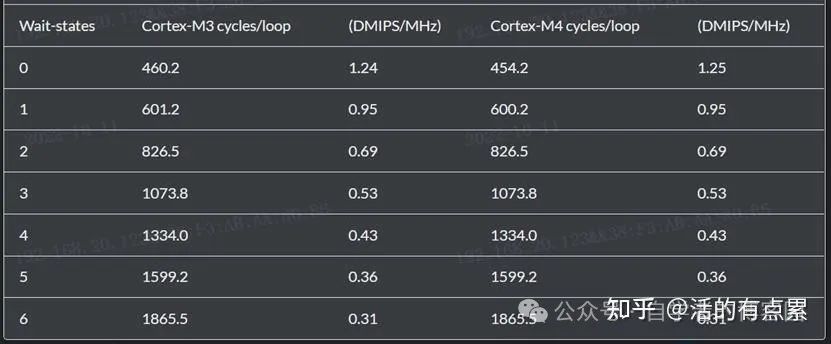
We can calculate that the DMIPS/MHz for Cortex-M3 at Wait-states 0 is:
DMIPS/MHz = 10^6 / (1757 * 460.2)= 1.2367 ≈ 1.24 DMIPS/MHz
The above calculation result corresponds to the data in the image. There is no DMIPS/MHz value description for Cortex-A76 on ARM’s official website, but it was found that when Cortex-A76 was released, ARM’s chief architect Filippo emphasized that the Cortex-A76 architecture has at least a 35% performance improvement over the previous generation (A75), and for some mathematical tasks, the new architecture processor can have a 50%-70% improvement.
Most online resources only go up to Cortex-A75, but the following DMIPS/MHz values for various architectures were found:
Arm Cortex-A75 5.2 DMIPS/MHz
Arm Cortex-A73 4.8 DMIPS/MHz
Arm Cortex-A72 4.7 DMIPS/MHz
Arm Cortex-A57 4.1 DMIPS/MHz
Arm Cortex-A55 2.7 DMIPS/MHz
Arm Cortex-A53 2.3 DMIPS/MHz
Although Qualcomm’s official website and product summary do not provide direct numerical descriptions of their products’ CPU computing power, by combining various online resources, we can estimate the real CPU computing power of Qualcomm’s SA8155P.
The CPU computing power of SA8155P is calculated as follows (assuming a 50% performance improvement based on A75, i.e., 5.2 * 1.5 = 7.8 DMIPS/MHz):
SA8155P computing power = 2.419GHz * 1 core * 7.8 DMIPS/MHz + 2.131GHz * 3 cores * 7.8 DMIPS/MHz + 1.785GHz * 4 cores * 2.7 DMIPS/MHz = 18868.2 + 49865.4 + 19278 = 88011.6 DMIPS ≈ 88 KDMIPS
This value has about a 12% error compared to the 100 KDMIPS computing power published by Quectel, but this was actually calculated using ARM’s method for Samsung’s processor. Samsung has optimized the ARM Cortex-A76 core, calling it the Kryo core, and with various hardware accelerators, it is speculated that Samsung’s performance optimization for A76 has exceeded a 50% performance improvement, reaching the median of the 50%-70% performance improvement described by ARM’s architect Filippo. Additionally, memory read/write speed and hardware acceleration engines may also directly affect CPU computing power performance.
Of course, it is also possible that some of the above data, information, or calculations are still not accurate. If anyone has more information or in-depth research, please point it out.
=================================================
GPU Computing Power
………….. To be continued, below is a summary of the chip composition information released by NVIDIA Thor:
In the field of autonomous driving, improving driving safety requires a synchronous increase in both the number and resolution of sensors. At the same time, more complex AI models are introduced (NVIDIA roughly has a qualitative leap in its products every two years). Safety is the primary criterion for robot development, requiring diversity and redundancy in sensors and algorithms. All of these require higher data processing capabilities.
NVIDIA has applied Grace, Hopper, and Ada Lovelace.
1. Hopper has an astonishing Transformer engine and rapid transformation of Vision Transformers.
2. The invention of multi-instance GPUs in Ada helps centralize in-vehicle computing resources while also reducing costs.
3. Grace is NVIDIA’s data center processor. Typically, all parallel processing algorithms are offloaded and accelerated by GPUs, so the remaining workloads are often limited by single-threaded performance, while Grace has excellent single-thread performance.
Thor’s internal Arm Poseidon AE core (automotive enhanced version). Thor supports connecting two chips through NVLink-C2C chip interconnect technology to run a single operating system (currently, many electric vehicle manufacturers are combining 2 to 4 Orin processors to meet computing power demands).
Thor can be configured in various modes, allowing its 2000 TOPS and 2000 TFLOPs to be fully utilized for autonomous driving workflows or configured to allocate part for cockpit AI and infotainment and part for assisted driving. Thor features multiple computing domain isolation, allowing concurrent, time-sensitive multi-process operations without interruption. It can run Linux, QNX, and Android simultaneously on a single computer. Thor centralizes many computing resources, reducing costs and power consumption while achieving a qualitative leap in functionality.
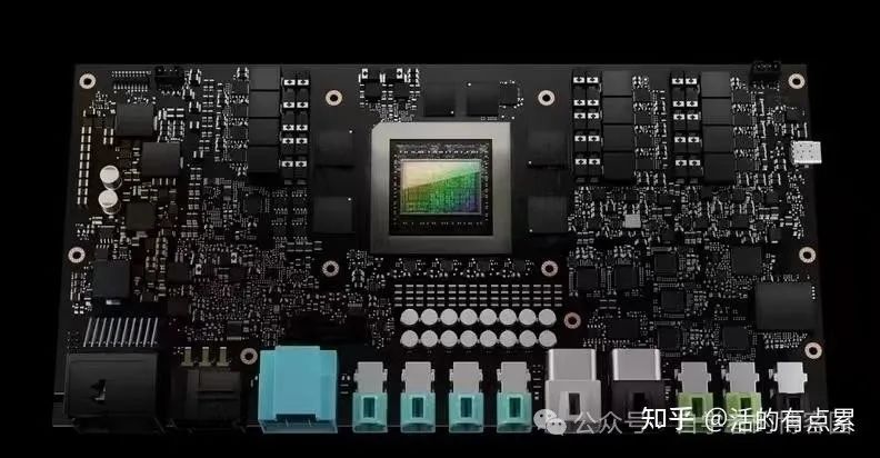
Releasing three years in advance is truly a challenge for NVIDIA, guiding numerous following IC manufacturers on the path forward.
Disclaimer: