A chip the size of a thumbprint, densely packed with billions of transistors, can be instantly destroyed by a careless touch. In the vast landscape of chip design, who is building a solid defense for this fragility? The answer lies in the pen and craftsmanship of layout engineers.
When discussing chip design, we are often eager to explore the intricacies of architecture, the efficiency of algorithms, and breakthroughs in performance—these are considered the “brain” and “soul” of the chip. However, whether a chip can stand firm in the real world and serve for a long time depends on a seemingly backend yet crucial aspect: physical layout design. The interplay between layout engineers and electrostatic discharge (ESD) protection is at the core of determining the chip’s “constitution” strength.
In the microscopic battlefield of micrometers and even nanometers, how do layout engineers weigh the immense weight of ESD to precisely layout defenses against invisible threats? Today, we dive into the microscopic world of chips to unlock the code of this silent guardianship.
1. The Invisible Blade: Why is ESD a “Formidable Opponent” for Chips?
To understand the mission of layout engineers, one must confront the lethal destructive power of ESD.
Electrostatic discharge (ESD) is essentially the process where a charged object (such as a human body or device) transfers static electricity to a chip through direct contact or electric field induction in an instant. This moment can be as short as nanoseconds to microseconds, but the voltage can soar to thousands or even tens of thousands of volts—enough to break through the most delicate structures inside the chip.

Human static discharge penetrating the internal structure of the chip
This instantaneous energy shock can cause two types of damage to the chip, both of which can be fatal:
1. Catastrophic failure: A massive energy surge directly melts metal connections and breaks through gate oxide layers, resulting in permanent loss of chip functionality, known as a “fatal blow.” A certain new energy vehicle company’s early BMS module (battery management system) suffered from a failure because the power rail was not isolated from the ESD discharge path. When maintenance personnel plugged and unplugged connectors, a ±8kV contact discharge caused the MCU input pin to break down, directly leading to communication interruptions and a collection accuracy deviation exceeding 10%.
2. Potential failure: Damage is more insidious, appearing normal during testing but gradually leading to performance degradation during long-term use.
A certain consumer-grade chip experienced frequent crashes after six months of use due to strong coupling between ESD devices and the core circuit substrate. Failure analysis revealed that it was due to hidden substrate damage caused by ESD that continued to spread.
This also means that without reliable ESD protection, the yield, reliability, and market competitiveness of the chip cannot be discussed. Moreover, over 70% of the ESD protection capability of a chip is determined during the layout design phase.
2. From Blueprint to Reality: The “Ideal” and “Implementation” of ESD Protection
Circuit design engineers typically provide mature ESD protection circuit solutions, such as classic GGNMOS, SCR, and other structures. These solutions are perfect on schematics, outlining the ideal path for low-resistance discharge. However, this is not the end; it is the starting point for layout engineers to transform the “paper blueprint” into “silicon reality.”
The core mission of layout engineers is to translate abstract circuit logic into manufacturable and effective physical structures on silicon. The effectiveness of ESD protection is precisely redefined in this “transformation” process.
Here lies a core contradiction: circuit design pursues “functional correctness,” requiring only logical connectivity and device size compliance; layout design must achieve “performance realization,” where details such as whether the wiring is symmetrical, whether the current density is uniform, and whether parasitic effects are controllable—these physical details directly determine whether the ESD protection circuit can withstand shocks at critical moments.
A certain chip once used a classic GGNMOS protection circuit, and the schematic verification showed a protection level of HBM 8kV, but during layout design, to save area, the originally integrated ESD device was split into two discrete units placed separately. As a result, after tape-out, it could only withstand 2kV of electrostatic discharge, because the ESD current concentrated through the first device, causing local burnout, while the second device hardly participated in the discharge—no matter how good the circuit solution is, it can completely fail due to layout errors.
3. The Practical Principles of Layout Engineers for ESD Protection: Five Core Principles
Integrating ESD protection into every detail of the layout requires layout engineers to adhere to five core principles, meticulously crafting in the microscopic world——
Principle 1: Balanced Current Distribution— Avoiding the Trap of “Current Congestion”
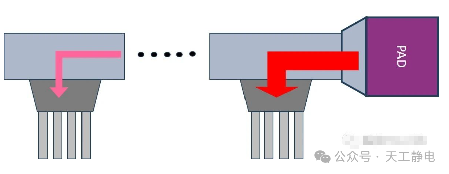
The ESD current is essentially a burst of massive energy flow, and the key to layout design is to allow this energy to flow evenly through multiple parallel finger transistors in the ESD protection device.
A certain chip initially adopted a single-sided contact fork structure, and the Finger Width design was below the foundry’s ESD Rule limit. During an ESD impact, only three finger transistors near the current entry opened, and they melted instantly due to excessive current density; subsequent adjustments were made to a symmetrical layout of dual-ring dummy fingers, allowing twelve finger transistors to conduct simultaneously, distributing the current evenly, and increasing the ESD withstand voltage from 1.5kV to 6kV, while the total width of the device did not increase.
Principle 2: Taming Parasitics— Dissecting the “Invisible Arrows”
Parasitic resistance and parasitic inductance in the layout are the “invisible arrows” of ESD protection. In a certain vehicle-mounted ECU PCB layout, the distance between the ESD device and the connector was 8mm, and the parasitic inductance introduced by a 35μm copper trace reached 40nH. During a 12.5A ESD current impact, the additional voltage drop exceeded 500V, directly breaching the core circuit’s tolerance limit. Subsequently, following the “3mm distance principle” to shorten wiring, the parasitic inductance was reduced to 1.5nH, and the additional voltage drop decreased by 70%. This also confirms the core strategy of layout design: widening metal lines to reduce resistance, prioritizing the use of thick upper metal layers for critical wiring, and minimizing the distance from ESD devices to pads.
Principle 3: Respecting the Rules— Not Just the Bottom Line of DRC
The design rule check (DRC) provided by the foundry is the “minimum standard” for manufacturability, not the “optimal criteria” for ESD protection. A certain 14nm process chip had excessively long high-speed I/O metal wiring and did not include antenna diodes. During the photolithography stage, the charge collected by the metal lines directly broke down the connected thin gate oxide transistors, leading to a yield drop of 12%, which was later mitigated through jumper design.
For ESD areas, layout engineers must adhere to stricter “ESD Rules,” such as the distance from the active area of the ESD device to the well edge and contact hole density requirements, which are usually much higher than for ordinary devices, aimed at enhancing device robustness.
Principle 4: Module Isolation— Building a “Safety Moat”
Excellent layout design relies on clear “functional partitioning” thinking. A certain company’s RFID chip laid out an independent protection ring between the core circuit and the I/O/ESD area, while also incorporating the chip’s outer seal ring into the ESD discharge path.
This design not only resists latch-up effects but also isolates noise, ensuring that ESD current discharges along the preset path without invading the core area, ultimately raising the chip’s ESD protection level from the industry standard of 6kV to over 10kV.
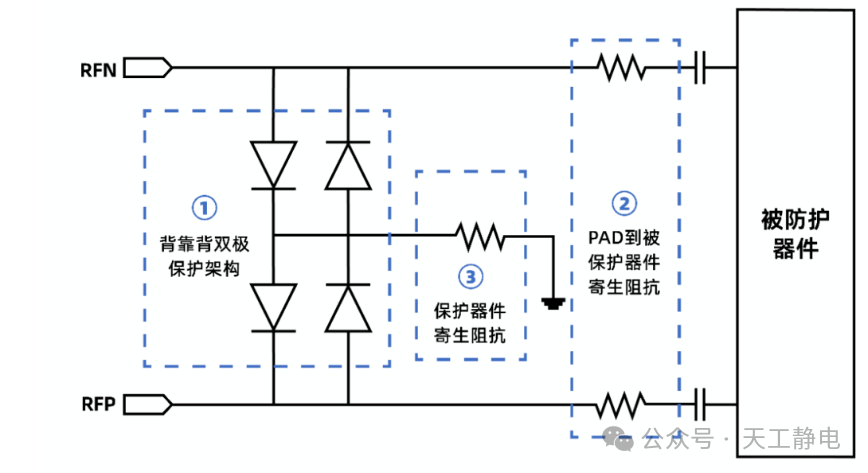
Three-dimensional ESD protection system schematic
Principle 5: Simulation Verification— Weaving the Final “Safety Net”
Completing the layout is not the end of the work. A certain HDMI 2.1 interface chip initially did not perform ESD post-simulation, and the parasitic capacitance of the ESD device in the layout was too large, resulting in a 40% eye height attenuation at a 12Gbps rate, exceeding the error rate limit.
Subsequently, by extracting the parasitic parameters (RC) from the layout and feeding them back into circuit simulation, the layout of the ESD device and wiring length were optimized, ultimately restoring the eye diagram template margin to 25%, meeting transmission requirements. This also indicates that post-simulation and PERC special checks are key to identifying vulnerabilities in discharge paths.
4. The Path to Advancement: The Delicate Balance of Performance, Area, and Reliability
Layout design has never been a one-way pursuit of perfection; it is an art of delicate balance. A certain 7nm FinFET process’s 28Gbps SerDes interface faced the pain point of “strong protection leading to excessive area.” Ultimately, engineers adopted the Sofics DTSCR local clamping structure, optimizing the layout to reduce parasitic capacitance to below 80fF, achieving a CDM 500V protection level with only a 3% increase in chip area. Behind this is the result of deep collaboration between engineers and circuit designers—they need to understand the chip’s application scenarios and find the optimal solution between the conventional protection of consumer electronics and the stringent requirements of automotive electronics.
Conclusion: Layout Engineers—The Ultimate Guardians of Chip Reliability
As Moore’s Law continues to delve into the nanoscale, the electric field strength within chips becomes increasingly concentrated, and device structures become more fragile, the requirements for ESD protection become more stringent. The role of layout engineers has evolved from mere “draftsmen” to “reliability designers” of chips.
Understanding the lethal threat of ESD means they must embed the gene of “reliability” into the physical texture of the chip through the arrangement of every metal line and the positioning of every contact hole.
Mastering the complex relationship between layout and ESD requires them to possess both the meticulousness of the microscopic world and the global vision of macro layout—being rigorous scientists adhering to physical laws and creative practitioners strategizing within confined spaces.
When a chip completes its long journey through design, manufacturing, and packaging, ultimately reaching the hands of users, it can withstand every accidental touch in the real world and operate stably in electronic devices for years or even decades—this is the highest tribute to the work of layout engineers. They are the behind-the-scenes artisans who forge the “golden shield” of life for chips.