Micro-nano manufacturing
Click to subscribe
When it comes to the semiconductor industry, many people’s first reaction is that there are still many products that are “stuck” domestically.
Do we always say we are restricted because we cannot produce similar products at all?
Of course not.
However, it is undeniable that we still have room for improvement in terms of precision control and competitiveness in some products.
With the iteration of femtosecond laser technology, we have now achieved an aperture precision of up to ±1μm, and can also realize high consistency in massive microholes. These advantages effectively address the challenges of processing semiconductor process components domestically.
Today, we take the Shower head (gas distribution plate) as the research object to explore how femtosecond lasers assist in the localization of semiconductor process components.
1
|Shower head and other process components
The Shower head, also known as the gas distribution plate, gas distribution disk, or spray head (hereinafter referred to as the gas distribution plate).
Due to its many aliases and its seemingly unremarkable appearance, resembling a showerhead, it has led to a misconception among precision machining practitioners that it is “so easy”.
In reality, the processing requirements for the gas distribution plate are at the ceiling level. It has thousands of microholes evenly distributed on its surface, with diameters mostly between 0.2-1mm, and requires each hole’s precision, roundness, spacing, consistency, and wall smoothness to be perfect. If any one aspect is not perfect, the entire product is considered defective.
This is because the spray head is a core gas distribution device that runs through key processes such as cleaning, etching, and deposition in semiconductor manufacturing, directly determining the process precision of the entire equipment.
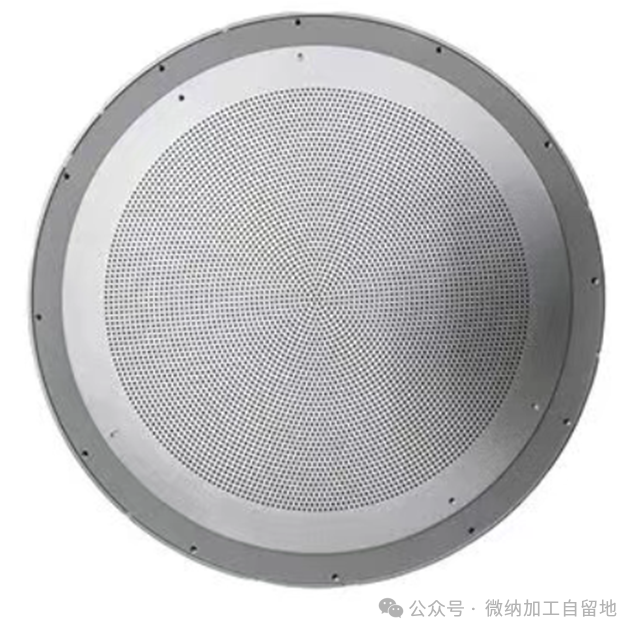
(Image source: Internet)
2
|Types of gas distribution plates and the current domestic processing situation
Since semiconductor processes may involve some extreme working environments, such as high temperatures, high pressures, or corrosive conditions, the material selection for the gas distribution plate is particularly important. Therefore, we can classify gas distribution plates based on material types.
Common gas distribution plates include metal types, such as aluminum alloys, stainless steel, and nickel. Among them, aluminum alloys are widely used due to their good thermal conductivity, corrosion resistance, and ease of processing. With the breakthroughs in femtosecond laser processing of more materials, the selection of materials for metal gas distribution plates will become broader.
Non-metal gas distribution plates are commonly made from corrosion-resistant, high-hardness, and brittle materials like silicon and ceramics. Traditional processing methods for these materials face issues such as edge chipping and low efficiency. The non-contact, minimal thermal impact advantages of femtosecond lasers can perfectly solve the precision processing challenges of these difficult-to-process materials.
According to reports, current international suppliers of gas distribution plates and similar components mainly come from abroad, such as the United States, South Korea, and Japan, whose products occupy a large share of the global market for similar products.
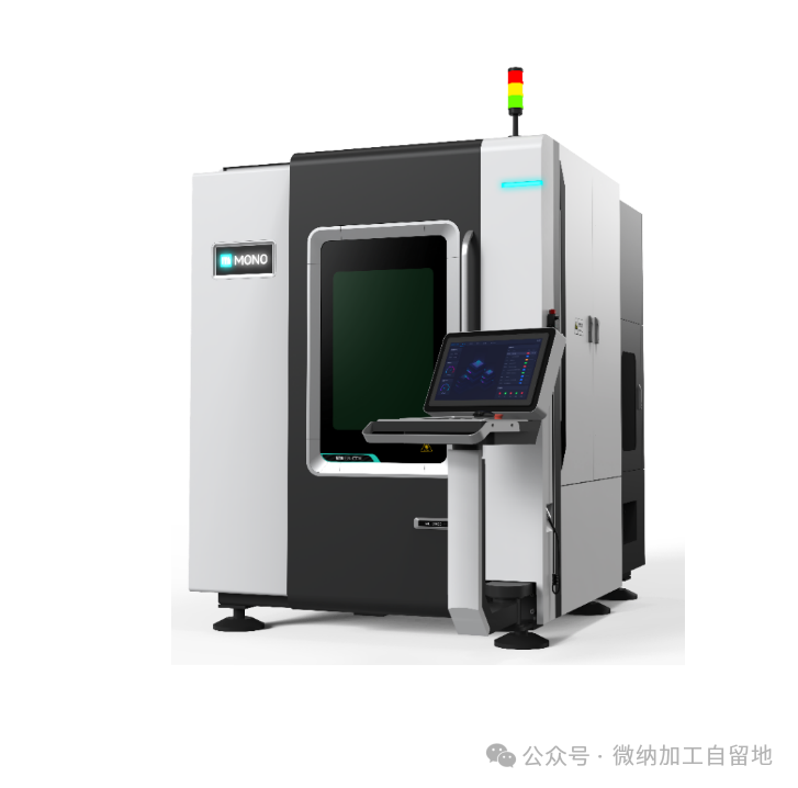
Based on this, some domestic large manufacturers specializing in precision processing or semiconductor component development are also researching this type of device. However, due to constraints such as familiarity with process technology and differences in processing equipment precision, we still need to invest a lot of effort in the development and production of high-end gas distribution plate components.
Therefore, the high-level iteration of processing technology has become a way to solve these challenges.
3
|Femtosecond laser microhole processing technology
As a cutting-edge laser processing technology, femtosecond lasers have been validated in the precision manufacturing of components in various fields such as semiconductors, aerospace, precision medical devices, and scientific instruments due to their high precision, high stability, non-contact processing, and minimal thermal impact.
Microhole processing is one of the problems that femtosecond lasers excel at solving.
Microhole processing involves many critical indicators, such as: hole diameter precision, roundness, positional accuracy, edge quality, wall roughness, heat-affected zone, consistency, hole spacing, verticality, and aspect ratio. For semiconductor process components like gas distribution plates, these indicators are equally important and interrelated, requiring simultaneous satisfaction of roundness, hole diameter precision, positional accuracy, consistency, edge quality, and other requirements.
Femtosecond lasers possess the capability to meet all of the above indicators simultaneously.
For example:
(1) Dimensional limits: Femtosecond lasers can achieve vertical holes as small as 20μm;
(2) Hole diameter precision: Femtosecond lasers can achieve ±1μm hole diameter precision, and this is not for a single hole, but the average hole diameter precision of all massive microholes can meet this range;
(3) Wall thickness: Femtosecond lasers can achieve very small wall thicknesses, such as 15μm, with no connected or broken holes in massive microholes;
(4) Consistency: Due to precise energy control, femtosecond lasers can achieve roundness consistency in massive microholes.
In addition to the above microhole indicators, femtosecond lasers maintain good equipment stability during continuous processing over dozens or hundreds of hours, significantly improving the yield of gas distribution plate processing and avoiding potential risks associated with other processing methods.
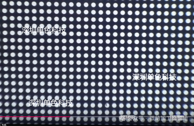
(Case of massive microhole processing)
4
|Conclusion
From the perspective of processing technology and market, the battle for semiconductor process components is not about price, but about precision, stability, and innovation.
The road is long and arduous, but we must work together.
We hope that through the continuous iteration of our femtosecond laser technology, more domestic semiconductor component developers and processors can achieve continuous breakthroughs.
-END-
Author: Chen Minlan (Femtosecond Laser Practitioner)
For more discussions on femtosecond laser micro-nano processing, feel free to reach out.