(Source: AI Jiwei)
Chip design is hailed as the most intricate yet grandest engineering endeavor in human history. After decades of development, advanced chip developers can integrate hundreds of billions of transistors into chips smaller than a fingernail. Their ability to achieve this goal relies on Electronics Design Automation (EDA) tools, commonly known as EDA tools.
EDA is the highest-end industry in the electronics sector, driving chip design, manufacturing, and end applications. From another perspective, any downstream innovation is inseparable from the innovative support of EDA software.
Depending on the application scenario, the use of EDA tools is mainly divided into several categories, including design, verification, and manufacturing. Chip design can be divided into front-end (logic design) and back-end (physical design) based on physical realization. Throughout the implementation process, the design will continuously be optimized, which may change the logical description method and structure, introducing the risk of errors. Therefore, verification runs through the entire design process, repeatedly ensuring that the logical optimization process does not alter functionality, timing meets target requirements, and physical rules are adhered to, resulting in a large number of verification processes and collaborative efforts from multiple parties.
In other words, verification is the most critical aspect of the chip development process.
Ubiquitous Verification
The chip verification process generally includes requirement definition, functionality realization, logic synthesis, and physical realization. Specifically:
Requirement definition mainly proposes the next-generation product requirements based on market analysis results. By combining external environment analysis, supply chain resources, and the company’s positioning, the application side presents the requirements for the new generation of products and further considers the product’s role, functionality, required board quantity, and types of integrated circuits needed, precisely defining product requirements.
Functionality realization describes the goals that the chip is expected to achieve. Developers use Verilog or VHDL and other hardware description languages to write millions of lines of code to implement chip functionality. Just like architectural design requires planning room numbers, purposes, and compliance with regulations.
Functionality verification involves iterative validation to make the design precise and reliable. Before chip manufacturing, errors in system software and hardware functionalities are identified through checks, simulations, and prototype platforms, optimizing performance and power consumption to ensure the design is accurate, reliable, and meets the originally planned chip specifications.
Logic synthesis is the transition from behavioral description to circuit-level description. After specification design and verification, developers convert the hardware description language into a logic circuit diagram, a step known as “logic synthesis.”
Physical realization involves creating the chip layout. This step transforms the logic circuit into a circuit diagram with physical connections, reasonably laying out and routing hundreds of billions or trillions of devices and circuits to avoid interference.
The physical layout is delivered to the wafer factory in the GDSII file format, where actual circuits are created on the silicon wafer, followed by packaging and testing, resulting in the chips we see. Current verification must almost permeate every step of chip design so that the chip R&D team can promptly identify errors. Only through thorough simulation and verification can the success and quality of the tape-out be ensured.
The verification stage brings many benefits to chip design, such as shortening chip design time and reducing chip design costs. Specifically:
First, regarding the complexity of chip design, as design and process technologies continue to develop, the scale of integrated circuit design becomes larger and more complex.
To shorten the time to market and save development costs, SoC (System on Chip) designs that integrate microprocessors, analog IP cores, digital IP cores, and memory (or off-chip memory control interfaces) have become mainstream. The challenge that comes with this is that the complexity of verification exhibits exponential growth. The goal of verification tool innovation is to complete increasingly complex verifications quickly, accurately, comprehensively, and easily debuggable, giving developers confidence to Signoff the design for tape-out to the wafer factory.
Developing a medium-scale chip typically requires a team of over ten people for more than a year and a half, while today’s mainstream SoC chips require an experienced team to invest 3-5 years in development. Therefore, an efficient verification platform is crucial for rapid convergence of verification.
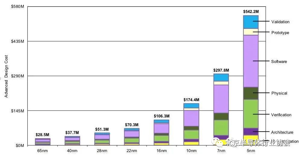
Secondly, regarding chip costs, recent data shows that the costs of advanced process chip design are extremely high, ranging from tens of millions to hundreds of millions of dollars. Design or process defects can easily render chips as “bad chips,” and re-taping not only incurs exorbitant financial costs but also delays the time to market by at least six months, risks that are unacceptable for commercial companies. Therefore, it becomes increasingly important to identify all design defects and errors through verification activities before tape-out.
Next, regarding safety, as chip usage scenarios extend to AI, cloud computing, smart cars, and 5G, the safety and reliability of chips have become unprecedentedly important.
We have completed the transition from scaled complexity to systemic complexity. When chips, systems, and software environments merge, countless “application modes” require thorough verification from a safety perspective. Taking the autonomous driving chips used in smart cars as an example, their complexity is no less than that of a small aircraft. The automotive industry requires systems to operate accurately to avoid dangerous situations and be capable of real-time monitoring and fault management.
Additionally, regarding hardware-software co-verification, in the early stages where software and hardware were not integrated, software and hardware development and verification were conducted independently, following a workflow of chip design and manufacturing followed by upper-layer software development.
Today, with the rapid development of AI, smart cars, and other fields, there is a new demand for dedicated chips and architectures that adapt to industry needs. Chips themselves are complex systems that combine hardware and software, requiring developers to define the need for hardware-software co-development from the requirement definition stage to achieve the desired functionality and performance.
Developers have introduced ESL (Electronic System Level) design concepts, which allow software development to only require programming models without needing hardware implementation details. In the early stages of design, a high-level abstract virtual prototype is constructed. Since hardware description details are not required, the simulation speed of system-level models is several orders of magnitude faster than RTL level simulations, enabling hardware and software personnel to utilize the system for hardware reference and software development in the early stages.
This concept is also a practice of the “Shift-Left” methodology, allowing relevant software development verification work to be completed before RTL implementation. Software can solve safety issues, but software itself also has safety issues. Therefore, once completed, software security must be checked to identify and continually resolve issues.
Especially in cases where we use a lot of open-source software, open-source can lead to data leakage issues. Therefore, we need to intervene in the earliest stages of the entire development process and address these issues in subsequent development, achieving Shift Left, accelerating chip development, reducing risks, and shortening the time to market.
Finally, regarding low-power design, low power consumption has always been a key requirement for portable electronic devices. In recent years, this requirement has expanded to many types of end products. Whether it is large-scale chip designs for autonomous driving or compact IOT chip designs, low power consumption is one of the important indicators that developers focus on.
The electronics industry has developed extensive power management technologies and defined a unified power format (UPF) to describe the design intentions of some of the most commonly used methods. The successful development of low-power semiconductor designs includes checking UPF descriptions and verifying UPF at multiple stages of the project. The corresponding metrics in chip development are PPA (Performance, Power, Area), where developers always focus on balancing these three important indicators during the design and verification process.
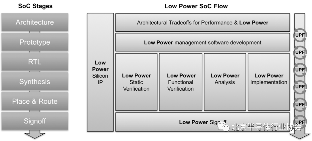
Low-Power SoC Design Process
In SoC design, using gate-controlled power and gate-controlled clock technology has become the most widely used and efficient method for power savings. Gate-controlled power relies on shutting down unused modules to save power, while gate-controlled clock reduces power by shutting down modules and registers that do not need to be activated. Therefore, developers achieve low-power requirements by setting dozens of voltage domains and thousands of power modes, while verification needs to ensure that the circuit behaves correctly in all power modes, the complexity and verification load of which can be imagined.
History of Verification Tool Development
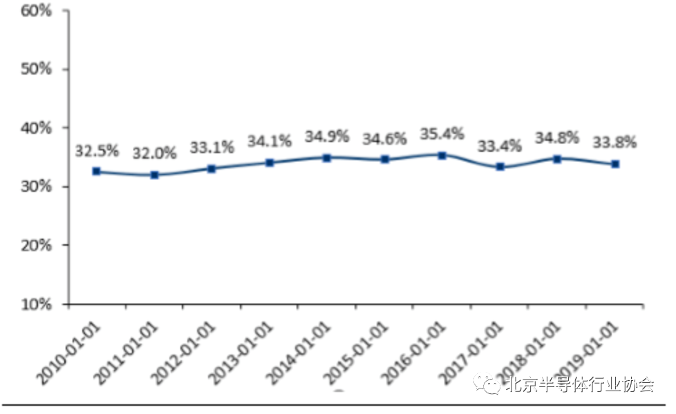
As mentioned earlier, design and process technologies are continuously evolving, making chips more complex. EDA tools are tied to processes, and every time semiconductor processes are updated, EDA must follow suit. It is understood that industry giant Synopsys invests up to 35% of its R&D expenses to maintain its industry position and keep up with technological developments. This clearly demonstrates the rapid pace of EDA development, and verification tools have also rapidly evolved.
Looking back at the history of verification tools is a story worth exploring.
It is important to note that the verification of digital circuits has gradually become more refined with the development of integrated circuit design and manufacturing, forming a significant branch of a vast skill tree that includes system-level verification, hardware logic functional verification, mixed-signal verification, software functional verification, physical layer verification, timing verification, and more.
Therefore, when reviewing its development history, it generally starts with the emergence of the Verilog language for hardware description used in the 1980s and the corresponding logic simulators. This article focuses on introducing two verification tools that have become new necessities along with the development of integrated circuits.
(a) Hardware Simulation
In the 1980s, all early hardware simulators were built using a large number of commercial FPGAs. These FPGAs were often thousands in number, installed on large boards housed in large cabinets, interconnected via complex FPGA backplanes, and connected to the target system through numerous cables to achieve input/output for the simulator. This deployment scheme was called ICE (In-circuit-emulation), which was cumbersome, unreliable, and time-consuming. The industry thus coined the term TTE (Time To Emulation) to express and measure the time spent deploying designs into the compiler and simulator; the reasons for its lack of promotion also included high ownership costs and the need for a team of experienced application engineers to support its deployment due to poor equipment reliability.
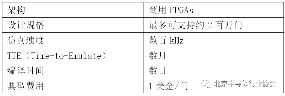
In around 1995, early hardware simulators featured
Simulation pioneer Quickturn collaborated with IBM in the 1990s to introduce new technologies to address shortcomings such as poor debugging capabilities, long deployment and compilation times, and performance that could not linearly scale with design size; in 1999, a company founded by Chinese individuals in Silicon Valley, Axis, launched an accelerator that allowed designs to be switched from simulators to proprietary simulators for debugging; in 2000, four French engineers founded EVE (Emulation Verification Engineering) and introduced a simulator called Zebu for Zero-Bugs.
By around 2000, hardware simulators had significantly improved through a new architecture based on custom ASICs, supporting software improvements, Verilog, and VHDL languages, and designed new deployment models. The customer base expanded beyond processors and graphics markets, with total capacity expandable to 100 million gates in multi-chassis configurations, achieving simulation speeds close to 1 MHz.
Today, as chip integration increases, SoC has gradually become the norm. By around 2015, designs had reached scales of billions of gates, and hardware simulation became a foundational tool for all verification strategies in SoC design. During this period, several mergers and acquisitions occurred, leaving only three companies competing in the simulation field: in 1998, Cadence acquired Quickturn and launched a hardware simulation system called Palladium; Mentor Graphics acquired Meta Systems and IKOS to launch the Veloce simulator and Questa®CodeLink; Synopsys acquired EVE in 2012 and launched the ZeBu-Server3 based on Xilinx Virtex-7 FPGA two years later.
(b) Virtual Prototyping
In the early days, developers wanting to verify their designs had to wait for extremely long simulation results or the results of tape-outs. If the results were not as expected, whether re-simulating or re-taping would incur extremely high costs. Therefore, when Xilinx and Altera launched reprogrammable gate arrays (FPGAs), developers began to verify designs by assembling effective flows using FPGA boards, which became a third option that was cheaper than tape-out and faster than simulation.
However, self-assembly means that designs need to be partitioned. More signals are transmitted between various partitions on FPGAs, requiring pin multiplexing. The number of gates grows quadratically while the number of pins grows linearly, meaning each pin connects thousands of gates. This method requires engineers to have extensive knowledge of design and FPGAs as well as familiarity with FPGA tool flows.
Therefore, in 2000, a company founded in Sweden, Hardi Electronics, officially launched a prototype system based on FPGAs called HAPS, which can quickly assemble ASIC prototype systems in various ways, saving customers months of time in critical verification stages. In 2007, Synplicity acquired this company for $24 million, and Synopsys acquired Synplicity in 2008 for $227 million. HAPS has evolved through several generations, reaching HAPS-80 in 2015, which remains the fastest prototype verification acceleration platform in the industry.
Simultaneously, S2C was established in 2003 in Silicon Valley to address the demand for FPGA prototypes; Cadence launched its Rapid Prototyping Platform, now known as Protium, in 2011; and developers still utilize their extensive FPGA knowledge to assemble prototype systems independently.
What Verification Tools Does Chip Design Need?
Currently, verification tools have evolved into many categories. As the world’s leading EDA solution provider, Synopsys has the most comprehensive tool product line, continuously developing tools suitable for complex chip systems, making Synopsys the focus of our research.
Before categorizing the tools, we must mention the recently popular AI technology. McKinsey Consulting predicts that AI is opening the best opportunities for the semiconductor industry in decades, as AI can help semiconductor companies achieve up to 40%-50% of value from their technology stack, while the mobile era only provided 20% of value. Synopsys’ AI laboratory director, Liao Renyi, has also pointed out that the ultimate form of EDA in the future is AI.
Recently, Synopsys launched the industry’s first AI autonomous chip design solution, DSO.ai, which reportedly can search optimization targets within the vast solution space of chip design tasks and complete designs rapidly. This is one of Synopsys’ significant achievements in applying AI to chip design technology over the years.
Returning to verification tools, it is evident that AI plays a significant role in this area. Verification tools are generally divided into architecture design, hardware development, software development, and the industry’s fastest hardware accelerators for simulation.
(1) Architecture Design: Exploration and Optimization
In architecture design, chip design first defines the system architecture, clarifying functionality, communication protocols between selected IP cores, and the balance of PPA (Power-Performance-Area).
AI chip design requires architectures with high performance and energy efficiency, which often represent more innovative architectures. In the early stages of architecture exploration and optimization, quickly building accurate architectural concept models verifies that system performance and power design goals can be achieved, helping neural network architects and algorithm designers rapidly determine a comprehensive and balanced architecture, eliminating risks of later changes in chip design, discovering issues early, and improving development efficiency, becoming a common demand in AI chip design.
As early as 2018, AI chip startup Cambricon announced that the verification tool used for its cloud intelligent processor chip was Synopsys’ HAPS prototype verification solution.
In fact, there are several chip companies like Cambricon that are using Synopsys design tools. Takashi Abe, project manager of the basic electronics R&D department at Denso, stated: “Automotive AI chip design requires architectures with high performance and energy efficiency. Platform Architect Ultra enables us to quickly build accurate architectural concept models and test them with actual AI workloads, effectively comparing hundreds of architectural and IP alternatives to ensure our automotive chips deliver optimal performance and efficiency.”
It is reported that Platform Architect Ultra is designed for intelligent mapping and optimization of AI chip architectures’ CNN, meeting the balance of high performance and low power consumption. Its unique technology, features, and AI reference systems support the integration, analysis, and optimization of AI architecture CNN workload models. AI chip teams can leverage Platform Architect Ultra for accurate and effective architectural trade-off decisions to eliminate later changes in chip design.
(2) Hardware Development: Static Checks and Formal Verification
In the early stages of the design process, quickly analyzing the synthesized netlist and checking whether the RTL design is functionally equivalent to the HDL design ensures that functionality has not been altered during optimization. Most defects can be identified and repaired before simulation, improving simulation speed and efficiency while reducing overall costs, time, and effort. Synopsys‘s SpyGlass and formal verification solutions are built on next-generation databases and engines, providing the necessary functionality and performance for verifying the largest and most complex designs.
Recently, Synopsys announced the launch of the VC SpyGlass™ RTL static Signoff platform, which employs the recognized SpyGlass® technology and is part of the Verification Continuum™ platform.
In this regard, Hideyuki Okabe, director of digital design technology, shared R&D, IoT, and infrastructure business units at Renesas Electronics, stated, “Insufficient or incorrect constraints are the primary causes of numerous violation issues, which correspondingly increase our debugging cycles. With the new machine learning technology in VC SpyGlass, our design team can significantly reduce the number of false positive CDC violation reports to accelerate root cause identification.”
(3) Hardware Development: Dynamic Simulation and Debugging
Simulation verification tests the correctness of code designs, with the standards being the specifications established in the first step. It checks whether the design precisely meets all requirements in the specifications. Specifications are the gold standard for determining design correctness; any violations or non-compliance with specifications require redesign and recoding. Design and simulation verification is an iterative process until verification results show complete compliance with specification standards.
In this regard, Synopsys has also laid out plans. Synopsys launched an enhanced native integration of the Verification Continuum, achieving performance improvements across all verification engines, accelerating time to market for complex SoC designs.
In this regard, Liang Bin, vice president of Iluvatar, stated, “To gain a competitive advantage, we need a comprehensive solution to improve the verification process and shorten the time to market for high-performance AI solutions. Synopsys’ VC Formal control and data path applications, combined with VCS native compilation and Verdi unified debugging, allow us to identify useless code in minutes and verify complex 128 x 128 MAC in a day.”
(4) Software Development: Virtual Prototyping Design Platforms
Virtual prototyping design allows software engineers to start development months before hardware design completion and fully launch systems within days after silicon production. As chips closely integrate with application fields, software development based on virtual prototypes will become the norm, and tools that accelerate software development will become increasingly popular.
Pingtouge collaborates with Synopsys in this area. Dr. Meng Jianyi, vice president of Pingtouge, stated, “During the development of the Xuantie 910 processor, Synopsys’ HAPS-80 system helped us deliver the chip prototype to the software team within two weeks, providing great assurance for the early market launch of the Xuantie 910 processor.”
Ray Cornyn, vice president and general manager of the vehicle networking processor department at NXP, pointed out that Synopsys launched the VDK for the S32G vehicle networking processor, which helps automotive system developers leverage the advanced features of S32G to accelerate their software development, integration, and testing.
(5) The Fastest Hardware Accelerators in the Industry: Verification Acceleration and Hardware-Software System Verification Testing
Placing designs still at the RTL level into a reconfigurable virtual hardware environment allows verification speeds to increase by thousands of times, launching operating systems on RTL modules within hours, while also making hardware-software collaboration possible.
In 2019, Synopsys announced a multi-year agreement with AMD, utilizing its ZeBu®Server 4 simulation system to accelerate the verification of an increasing number of AMD high-performance processors, graphics, and gaming projects. In this regard, Alex Starr, a senior researcher in the simulation and rapid platform modeling department at AMD, commented, “The complexity of high-performance processors, graphics, and gaming chips continues to increase significantly. High-performance simulation has become a key component of our development strategy. Deploying ZeBu Server 4 enables us to efficiently analyze the energy efficiency and performance of new architectures and handle customer workloads.”
Summary
Verification is a crucial guarantee for chip development, accounting for over half of the chip development workload. It is a process of mathematically pushing errors to be infinitely close to zero. With the growing demand for chips in innovative application areas represented by AI, autonomous driving, and 5G, the challenges faced in verification work for different types of chips are becoming increasingly complex and diverse. The pairing of verification tools, scalability, and accelerating hardware-software development have become focal points for developers. Synopsys has already developed mature solutions for different fields to help clients shorten development cycles and improve tape-out success rates.