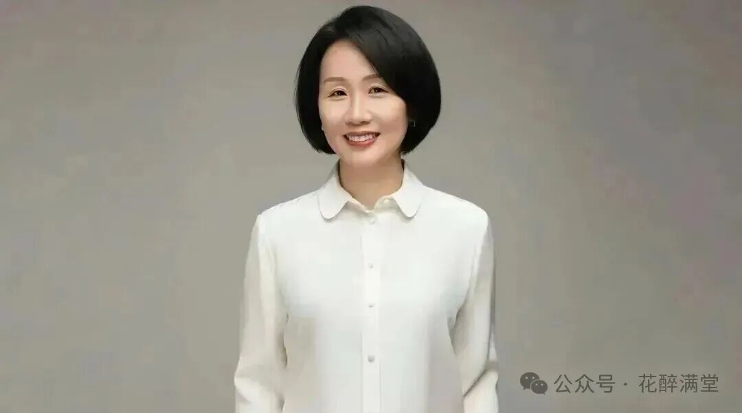
Innosilicon Founder Luo WeiweiAuthor | Qiu XinhaoSource | Qiu Chujian
In the summer of 2025, a list from NVIDIA’s supply chain caused a stir in the semiconductor industry.
Among the well-established manufacturers from Europe, America, and Japan, a little-known Chinese name appeared: Innosilicon.
From the Chief Scientist at NASA to the entrepreneur leading the global market in gallium nitride (GaN) power semiconductors, Innosilicon’s founder Luo Weiwei completed a breakthrough from 0 to 1 in just eight years.
As of September 23, 2025, Innosilicon’s market value has reached 87.5 billion Hong Kong dollars, making it the leader in the global GaN power semiconductor field.
All of this began with a decision in 2015 that was not well-received.
1
“Jumping into the Fire Pit”
In 2015, when Luo Weiwei decided to return to China to start a business, almost no one around her supported her choice.
Some even bluntly told her: starting a business in China is a “fire pit”, and she should not jump in. In the end, only one employee was willing to follow her back to China.
Luo Weiwei graduated with a PhD in Applied Mathematics from Massey University in New Zealand. After working for 15 years at NASA, she founded two high-tech companies focused on new materials.
With her industry insights, Luo Weiwei returned to China in 2015 with dreams of third-generation semiconductor gallium nitride.
At that time, the global development of third-generation semiconductors was still in its early stages, and gallium nitride had not yet been widely commercialized. What surprised the industry even more was that Luo Weiwei chose a different technical path—while most companies were still using 6-inch or 4-inch processes, she resolutely decided to tackle 8-inch silicon-based gallium nitride wafer technology.
This choice carried enormous risks and rewards. Compared to 6-inch silicon-based gallium nitride wafers, the yield of 8-inch wafers could increase by 80%, and the cost per device could be reduced by 30%. However, the difficulty of achieving this was exponentially greater, with professional assessments suggesting it could take 9 years to achieve mass production.
“Experience will not become a bottleneck or barrier to development.” With her fifteen years of experience at NASA, Luo Weiwei firmly believed that there are not many things in this world that cannot be accomplished.
In December 2015, Luo Weiwei established a company in Zhuhai, operating as a small-scale production base. As R&D progressed, production capacity gradually could not meet demand.In 2017, she officially founded Innosilicon in Suzhou, shifting towards large-scale industrialization.
Luo Weiwei led Innosilicon to overcome one technical challenge after another. The company not only became the first in the world to achieve mass production of 8-inch silicon-based gallium nitride wafers but is also the only company capable of mass-producing gallium nitride semiconductor products across the entire voltage spectrum.
This breakthrough filled a gap in the industry and improved the layout of China’s semiconductor industry chain.
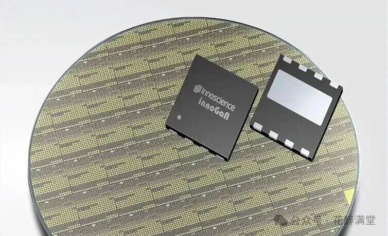
Compared to 6-inch silicon-based gallium nitride wafers, Innosilicon’s 8-inch wafers have a significant cost advantage, giving it a favorable position in market competition.
According to Frost & Sullivan, based on revenue in 2023, Innosilicon ranks first among global gallium nitride power semiconductor companies, with a market share of 33.7%. When calculated by the shipment volume of gallium nitride discrete devices, Innosilicon is also firmly in first place, with a market share of 42.4% in 2023.
Innosilicon’s products currently cover multiple fields including consumer electronics, renewable energy, industrial applications, automotive electronics, and data centers. Among them, sales of gallium nitride discrete devices and integrated circuits are growing rapidly, with revenue expected to increase by 87.8% to 361 million yuan in 2024, accounting for 43.5% of total revenue.
2
Capital Support
Before going public, Innosilicon completed five rounds of financing, totaling over 6 billion yuan. This figure is relatively rare among semiconductor startups in China.
Notably, in the C round of financing, CATL founder Zeng Yuqun personally invested 200 million yuan in Innosilicon. By the time of the IPO, Zeng had transferred this equity to his wife, holding a stake of 1.78%.
Innosilicon’s ability to attract such significant capital support is not only due to its leading technology but also because its products have wide applications in the new energy vehicle sector. In fact, in Innosilicon’s nearly 600 million yuan revenue in 2023, contributions from CATL accounted for over 30%.
Additionally, Luo Weiwei’s choice to establish the company in Suzhou was not coincidental.
Suzhou has been promoting the layout and implementation of integrated circuit design, manufacturing, packaging, and testing industries since 2002. Today, Suzhou has become one of the regions with the highest concentration and industrialization level of third-generation semiconductor resources in China.
“Opportunities always favor the prepared.” Suzhou’s long-term layout in the integrated circuit industry has made it an ideal place for Innosilicon’s development. From the initial funding for Innosilicon’s establishment in Suzhou to cornerstone investments for the IPO, Suzhou has provided strong support.

In December 2024, Innosilicon was listed on the main board of the Hong Kong Stock Exchange, with an issue price of 30.86 Hong Kong dollars/share, raising a total of about 1.4 billion Hong Kong dollars. This IPO attracted four cornerstone investors, including STMicroelectronics and Jiangsu State-owned Enterprise Mixed Reform Fund, with a total subscription amount of 100 million US dollars, exceeding half of the total IPO fundraising amount.
After going public, Innosilicon continued to expand its production capacity advantage.In July 2025, the company announced it would increase the monthly production capacity of 8-inch gallium nitride wafers from 13,000 to 20,000 wafers. Previously, Innosilicon had stated that it plans to increase monthly production capacity to 70,000 wafers within the next five years.
At the same time, Innosilicon announced a joint development agreement with STMicroelectronics to jointly promote the application of gallium nitride technology in consumer electronics, data centers, automotive, and industrial power systems.
According to the agreement, Innosilicon can use STMicroelectronics’ manufacturing capacity outside of China to produce its gallium nitride wafers, while STMicroelectronics can utilize Innosilicon’s manufacturing capacity in China to produce its own gallium nitride wafers.
This collaboration not only enhances Innosilicon’s supply chain flexibility but also reflects the recognition of its technical strength by international semiconductor giants.
3
Broad Prospects
Gallium nitride, as a leading third-generation semiconductor material, exhibits broad application prospects in electric vehicles, data centers, photovoltaic power stations, and other fields due to its advantages of high frequency, high voltage resistance, and high electron mobility.
According to Frost & Sullivan, it is expected that by 2028, the global gallium nitride power semiconductor market will reach 50.1 billion yuan, accounting for 10.1% of the global power semiconductor market.
Innosilicon’s products have already been widely applied in the new energy vehicle sector.
Its automotive-grade GaN chips have entered the supply chains of companies like BYD and NIO, covering mid-to-low power scenarios such as onboard laser radar and OBC (onboard charger).In the first half of 2025, Innosilicon’s automotive-grade chip deliveries increased by 128% year-on-year.
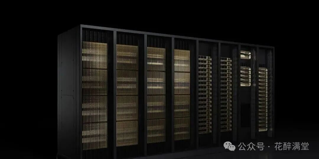
In the AI and data center sectors, after partnering with NVIDIA, Innosilicon will provide a full-link gallium nitride power solution for its 800V DC power architecture, positioning it to capture a market share of 20%-30% in the future data center power system renovation market.
Additionally, Innosilicon is also showing strong growth momentum in consumer electronics and humanoid robotics.
Although Innosilicon is currently still in a loss-making state, the loss margin is gradually narrowing. Financial reports show that the company achieved sales revenue of 553 million yuan in the first half of 2025, a year-on-year increase of 43.4%; net losses were about 429 million, a year-on-year reduction of 12.16%.
More importantly, the company’s gross margin is 6.8%, compared to achieving positive gross margins in the same period of 2024, indicating a significant improvement in profitability.
As the global third-generation semiconductor market enters a prosperous period, Innosilicon is ushering in a golden stage of development. Luo Weiwei stated that the company will continue to expand production capacity, strengthen R&D, and expand its global sales network.
This female scientist from NASA has already made a significant mark in the history of China’s semiconductor industry.
(End of article)
【About Qiu Chujian】
The author is from Longyan, Fujian, and is currently based in Beijing. The public account focuses on writing about the growth experiences and cognitive upgrades of business leaders, encouraging us to learn from them and continuously grow and evolve.