1. The Birth and Evolution of PCBs
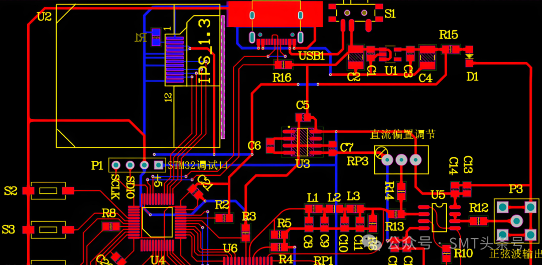
-
Prototype Stage (1903–1940) In 1903, German engineer Albert Hanson created “circuits” by sandwiching metal foil between wax paper in telephone switchboards, considered the earliest concept of “inter-layer interconnection.” In 1925, Frenchman Charles Ducas used templates to print conductive ink, proposing the concept of “printed wiring” for the first time.
-
Practical Application (1940–1950) World War II drove the miniaturization of military technology. In 1941, Austrian Paul Eisler used etched copper foil on an insulating board in a radio for the first time, creating the first functional PCB. In 1948, the commercialization of PCBs was officially approved in the United States.
-
Industrialization (1950–1970) · In the 1950s, transistors replaced vacuum tubes, leading to mass production of single-sided etched copper foil boards.
· In 1953, Motorola invented the plated through-hole method, giving birth to double-sided boards.
· In 1961, Hazeltine produced a 4-layer multilayer board, significantly increasing wiring density. -
High Density and Miniaturization (1970–2000) · In the 1970s, multilayer boards expanded to 6–12 layers, with line widths entering the 0.1 mm era.
· In the 1980s, surface mount technology (SMT) replaced through-hole technology, increasing board space utilization by over 30%.
· In the 1990s, high-density packaging such as BGA and CSP promoted blind/buried vias and HDI processes. -
21st Century: Advanced Packaging and System-Level Integration · After 2005, arbitrary layer interconnection (ELIC) and substrate-like PCBs (SLP) emerged, with line widths/spacing ≤ 20 µm.
· Since 2020, IC substrates, SiP, AiP, and module antennas have pushed PCBs into the “system-level interconnection” stage.
The Chinese Path Starting in 1956 → Mass production of single-sided boards in the 1960s → Introduction of foreign production lines in the 1980s → In 2003, production value surpassed that of the United States, ranking second in the world. By 2023, China accounted for 54% of the global PCB production value, with high-end substrates (ABF, FC-BGA) accelerating breakthroughs.
2. Main Types of PCBs
-
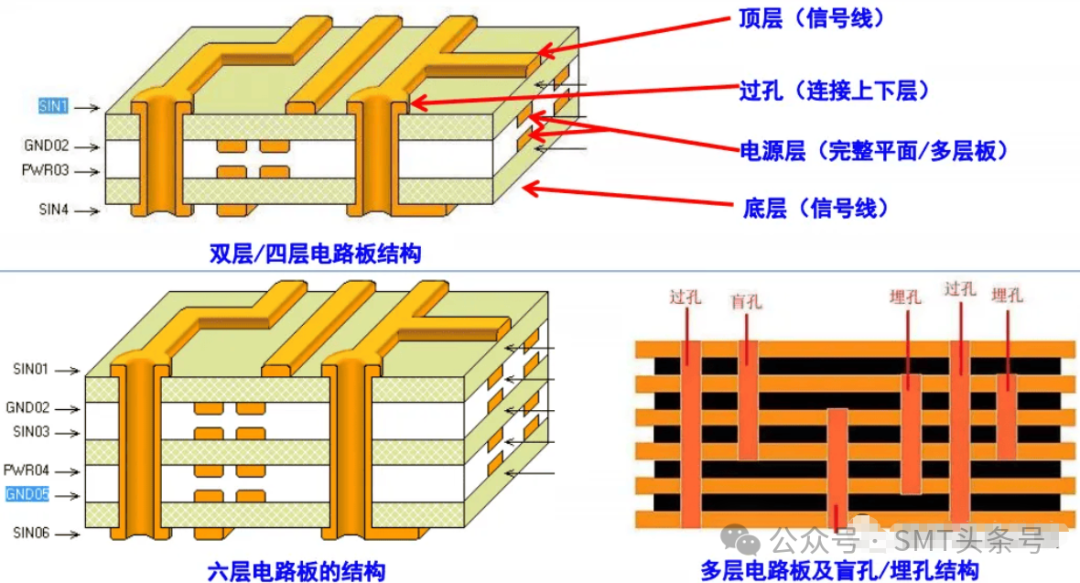
By Layer Count · Single-Sided Boards (SSB)
· Double-Sided Boards (DSB)
· Multilayer Boards (MLB, 4–120 layers) -
By Material · Rigid Boards: FR-4, CEM-3 epoxy glass fabric-based
· Flexible Boards: PI, PET film-based (FPC)
· Rigid-Flex Boards
· High-Frequency and High-Speed Boards: PTFE, LCP, PPE, and other low dielectric loss materials -
By Process Features · HDI: Laser micro-holes + plated through holes for higher density interconnection
· Metal Substrates (IMS): Aluminum-based, copper-based for LED heat dissipation
· Substrates (IC Substrate): Line width/spacing < 15 µm, supporting chips
· Thick Copper Boards (≥ 2 oz): High current power modules
· Backplanes: Communication base stations with 20–60 layers, board thickness of 4–8 mm
3. Functions of PCBs
-
Electrical Interconnection: Replacing manual wires with copper foil lines to achieve signal, power, and ground connections between components.
-
Mechanical Support: Providing a reference surface for component installation, withstanding vibration, shock, and thermal cycling.
-
Thermal Management: Reducing hotspot temperatures through copper layers, metal substrates, or embedded heat pipes/copper blocks.
-
Electromagnetic Compatibility: Reasonable stacking, impedance control, and shielding layers to suppress EMI/SI issues.
-
Miniaturization and System Integration: HDI, SiP, and AiP integrate “systems” into one or several boards, driving emerging industries such as 5G, AI, wearables, and electric vehicles.
4. Conclusion From brass riveted wooden boards in 1903 to 14 nm line width SiP substrates in 2025, PCBs have evolved from mere “circuit carriers” to the neural networks of modern electronic systems. With the advent of heterogeneous integration, chiplets, and 3D packaging, PCBs will continue to evolve towards thinner, denser, and smarter designs, playing a core role as the “mother of electronic products.”