
Click the image for details
As the preparations for the sixth Optoelectronic Integrated Chip Training are underway, we have received great news from the fifth Optoelectronic Integrated Chip Design Training Class: three excellent design solutions submitted by students have successfully completed tape-out. This training class has gathered outstanding students and researchers from across the country. Through a systematic training combining theoretical learning and practical operation, students have deeply mastered the full chain of skills in optoelectronic chip design, from basic theory to engineering practice. During the acceptance phase of the training results, the design works submitted by the students demonstrated exceptional technical levels and significant innovative capabilities, with three excellent design solutions successfully passing the rigorous review by the expert panel, earning valuable tape-out opportunities.
The three design solutions representing the training results in optoelectronic integrated chips successfully completed tape-out on April 27, 2025, and have recently been tested by their respective students. The success of this tape-out not only affirms the students’ abilities but also serves as a strong testament to the effectiveness of the training class, providing high-quality innovative talents and design results for the field of optoelectronic integrated chips.
The smooth completion of this tape-out work is attributed to the strong support from Shanghai Mingkun Semiconductor Co., Ltd. and the Shanghai Institute of Microtechnology, which provided technical platforms and resources, ensuring a solid guarantee for the final realization of the design solutions.
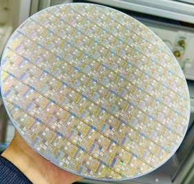
Figure 1: Silicon photonic MPW wafer containing the fifth Optoelectronic Integrated Chip Training Block

Highlights of the Training Class:
1. A Novel Photonic Integrated Circuit Based on All-Optical Recurrent Neural Networks (ORNN)
Completed by: Huang Xiaoan (Nokia Bell Labs)
Innovative Design: This group of students successfully designed a novel photonic integrated circuit (PIC) based on all-optical recurrent neural networks (ORNN). The core of the design lies in the use of a patented optical loop structure, ingeniously combining directional couplers (dc_in/dc_out) with a loop phase shifter, achieving significant breakthroughs in spatial utilization efficiency and signal processing capability. This design utilizes a low-space-occupying delay line, effectively reducing the chip size, and its optical loop architecture can support more complex all-optical signal processing tasks, functionally surpassing the limitations of traditional PNNs, and replacing high-energy-consuming DSP chips with an all-optical processing approach, achieving a leap in energy efficiency.
Measured Verification:
-
Insertion Loss (Figure 1): Measured value is 15.221 dB (transmitter 13dBm, receiver CH4 channel: -2.221dBm).
-
Function Comparison (Figure 2):
-
ORNN Scheme (4 delays + loop, red line): Successfully achieved all-optical correlation detection of 7-bit patterns.
-
Traditional PNN Scheme (4 delays, blue line): Detection function completely failed.
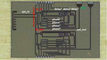
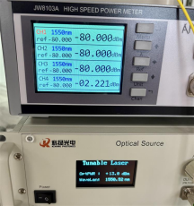
Figure 2: a) PIC test view of the proposed ORNN; b) The PIC probe station test: the CH4.
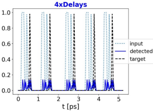
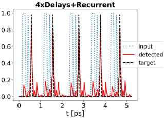
Figure 3: a) Performance evaluation of the prior time-delayed neural network with 4x delays; b) Performance evaluation of the proposal with 4x delays + recurrent.
2. 400G High-Speed Optical Module Prototype Chip
Completed by: Zhang Honghui (The Chinese University of Hong Kong), Zhang Honghui (The Chinese University of Hong Kong), Sun Wang (Nanjing University of Posts and Telecommunications), Chen Peiyu (Hong Kong University of Science and Technology), Wang Weixin (Sun Yat-sen University)
Innovative Design:
This chip is designed for next-generation optical communication systems, integrating a four-channel Mach-Zehnder modulator (MZM) architecture, supporting high-speed optical transmission of up to 400Gbps. Each channel is independently designed to achieve single-wave 100Gbps PAM4 modulation through high-speed traveling-wave electro-optic modulation technology. The chip operates in the O-band, providing high-density, low-latency transmission solutions for applications such as data center interconnects and 5G networks.
Measured Verification:
The total insertion loss of a single Mach-Zehnder modulator (MZM) is approximately 32 dB (including fiber array coupling loss and input light source splitting loss), extinction ratio (ER) is approximately 12 dB, and simulated bit error rate (BER) is about 10^-9.
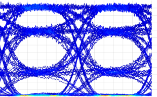
Figure 4: Simulated eye diagram
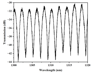
Figure 5: Measured MZM spectrum
3. High-Speed Micro-Ring Modulator
Completed by: Zhou Yuting (Tsinghua University)
Innovative Design: Innovations were made in the size structure of the micro-ring.
Measured Verification: This chip is developed for low-power, high-speed optical interconnect applications, supporting 100 Gbps On-Off Keying (OOK) modulation format.

Figure 6: Experimental measurement transmission spectrum
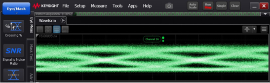
Figure 7: Experimental measurement eye diagram
The success of this tape-out is an important milestone in the professional growth of the students. We look forward to them gaining richer experience in subsequent testing and in-depth research. The sixth Optoelectronic Integrated Chip Design Training will be held from September 1-3, 2025, in Wuhan. We will continue to deepen the training philosophy of “promoting learning through practice and demonstrating capabilities through results,” optimize the curriculum system, strengthen industry connections, and provide a high-level growth platform for more aspiring students in the field of optoelectronic integrated chips, continuously delivering more outstanding innovative design talents for our country in this field.