0x01 Basic Overview
Fault injection is a side-channel attack technique that introduces a certain form of disturbance or invalid state into a system to alter its behavior. Typically, in embedded hardware and electronic devices, this disturbance can take various forms. Common methods of fault injection in electronic devices include:
– Clock glitch injection (imposing erroneous clock edges on the input clock lines of the IC)
– Voltage fault injection (applying a voltage above or below the expected voltage to the IC power lines)
– Electromagnetic interference (introducing electromagnetic disturbances)
This article will focus on voltage fault injection, particularly the introduction of transient voltages outside the normal operating conditions of the target device’s power supply. These transient pulses or input voltage drops (glitches) affect the operation of the device and achieve specific effects. Commonly expected effects include “corrupting” instructions or memory within the processor and skipping instructions. Previous studies have shown that these effects can be predictably achieved and have also provided some explanations for the EM effects that may arise from various behaviors (caused by glitches).
However, there is a gap in published research regarding the association of faults and related EM effects with specific state changes at the processor level (i.e., what exactly happens within the processor at the moment a fault occurs that causes instructions to be corrupted or skipped). This article aims to quantify and delineate the state of the processor before, during, and after fault injection, and describe discrete changes in marked states, such as registers (including general-purpose registers) and control registers (e.g., $ pc and $ lr), and memory.
Special thanks to colleagues at Toothless Consulting, whose excellent blog article series introduced me to fault injection and inspired this project. Thanks also to Chris Gerlinsky, whose research on the security of embedded devices, particularly his talk on breaking the CRP on LPC series chips, has been a valuable resource for this project.
https://toothless.co/blog/bootloader-bypass-part1/
https://recon.cx/2017/brussels/talks/breaking_crp_on_nxp.html
0x02 Test Setup
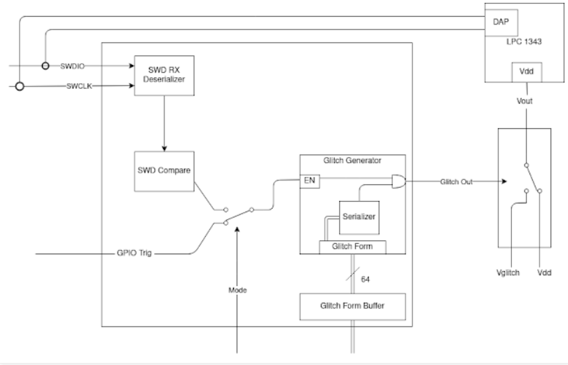
The target device selected for testing is the NXP LPC1343, which is an ARM Cortex-M3 microcontroller. To control the input target voltage and coordinate glitches, a Digilent Arty A7 development board based on Xilinx Artix 7 FPGA was used. Custom gateware was developed for the Arty board to facilitate the control and triggering of glitches based on various factors. For the purposes of this article, the two main triggers used are a GPIO line that synchronously goes high/low with certain device operations, and the SWD signal corresponding to a “step” event. The source code for the FPGA gateway software is [available here](https://github.com/Ethan-ks/glitcherPlatform).
https://github.com/Ethan-ks/glitcherPlatform
To switch between standard voltage levels (Vdd) and glitch voltage levels (Vglitch), a Maxim MAX4617 multiplexer IC was used. It is capable of switching between inputs in as little as 10ns, making it suitable for generating glitch waveforms on the LPC 1343 power rail with sufficient precision and timing.
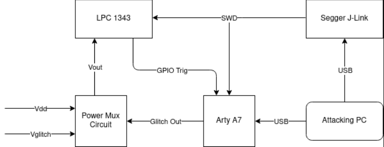
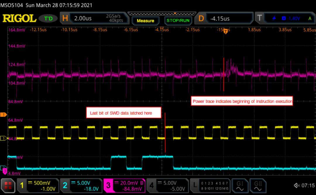
As shown in the figure above, the Arty A7 monitors the “trigger” line, which is either the GPIO from the target or the SWD line between the target and the debugger, depending on the operating mode. When the expected conditions are met, the A7 will “glitch out” according to the provided waveform specification, triggering the switch between Vdd and Vglitch via the power multiplexer circuit, feeding it to the target Vcore voltage line. A Segger J-Link is used to provide debug access to the target, and the SWD line is also fed to the A7 for triggering.
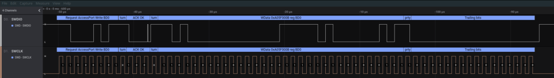
To facilitate triggering of any SWD command, a quasi-system SWD receiver was implemented on the A7. The receiver parses the SWD transactions sniffed from the bus and outputs deserialized headers and transaction data, which can then be compared against pre-configured target values. This allows triggering of the glitchOut line based on any SWD data (e.g., STEP and RESUME transactions), providing a timed glitch for single-step instructions.
Before performing any direct testing of faults during single-step instruction execution, observing the faults and their induced effects during normal operation helps to gain fundamental insights and provides a platform for hypotheses to be tested later. To provide an environment for observing the results of fault injection in various forms and durations, the program execution includes a simple loop that increments and decrements two variables. In each iteration, the value of each variable is checked against known target values, and when either condition is met, the execution will break out of the loop. Outside the loop, these values will be checked against expected values, and if they differ, they will be transmitted to the attacker’s PC via UART.
Using Binary Ninja reverse engineering software provides a visual representation of the compiled C. Since the provided assembly representation is generated from the machine code after compilation and linking, we can ensure it matches the behavior of the processor exactly (ignoring concepts like parallel execution).
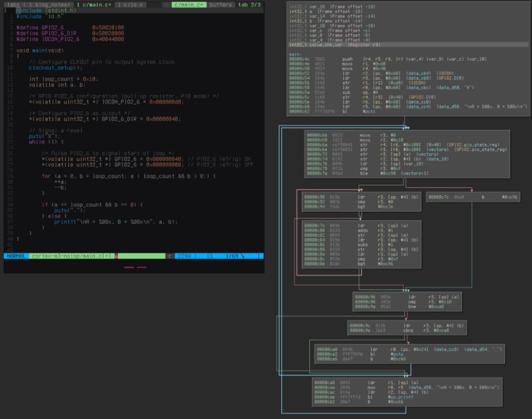
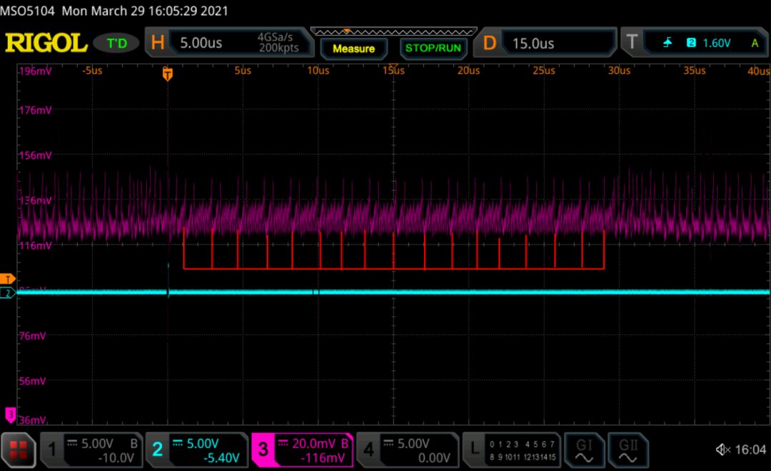
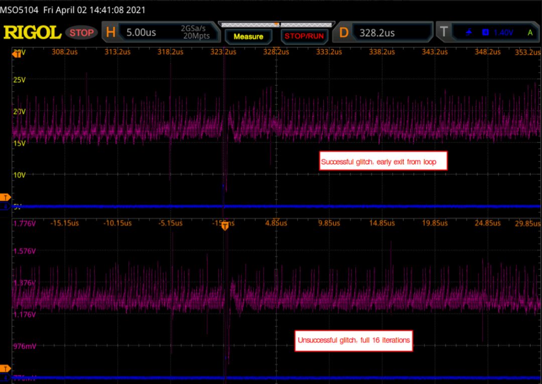
Although simple, this environment provides many interesting targets for fault injection. The loop includes memory access instructions (LDR, STR), arithmetic operations (ADDS, SUBS), comparisons, and branching operations. Additionally, the pulse from PIO2_6 provides the trigger signal for the glitchOut from the FPGA, which can target different areas/instructions throughout the loop based on the delay applied to that signal. The execution can be tracked using shunt resistors and transmission line probes to observe the power consumption of the ARM core.
The following waveform shows the GPIO trigger line (blue) and the power trace from the LPC (purple). The GPIO line goes high for one cycle and then goes low, marking the start of the loop. This is followed by a pattern repeated 16 times, indicating the 16 iterations of the loop. This is limited on either side by the power trace corresponding to the code used to write data to the UART and branches back to the start of the main loop.
The following content was obtained:
1. A reference of the actual instructions being executed by the processor (disassembled via Binary Ninja)
2. A visual representation of that execution, which can be viewed in real-time as the processor executes (via power tracking)
3. A means of taking action within the system under test, allowing calibration based on the behavior of the processor (FPGA glitcher).
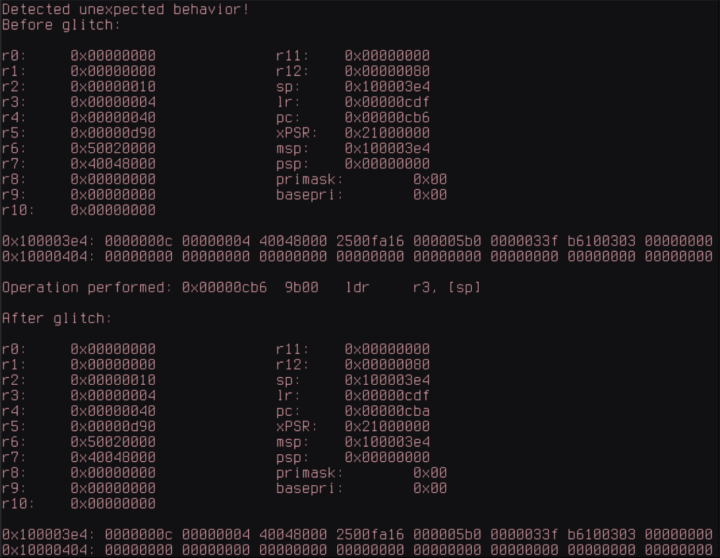
Using the above information, the offset between the fault and the trigger can be altered, and this timing can be (roughly) associated with a given instruction or group of instructions being executed. For example, by triggering a glitch at a certain time during the sixth repetition of the pattern on the power trace, we can observe that this part of the power trace seems to be cut off prematurely, and the value reported on the UART by the target reflects some malfunction or corruption during the sixth iteration of a certain loop.
So far, the approach taken has been consistent with traditional fault injection parameter search techniques, optimizing system visibility using certain behaviors inherent in device operations (the GPIO line pulse here) to determine the most effective timing and glitch duration. While this provides a rough understanding of the impacts of successfully injected faults (for the example above, we can assume that some operation during the sixth iteration of the loop has changed, but more specificity is merely conjecture), it could be other possibilities such as skipped load instructions, memory corruption, or comparison failures.
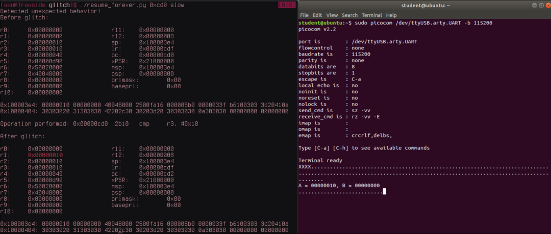
To illustrate this, below is a parsing, sorting, and counting output of UART traffic from the target device after running the external loop for thousands of iterations. The glitch delay and duration remain constant, but the discrete state impacts on variable states at the end of the loop are quite extensive. Some entries are easy to infer, such as the first and most common result: B is the expected value after six iterations (16-6 = 10), but A is 16, so the skipped LDR or STR instruction may have left a value of 16 in that register due to a previous operation. However, other results are difficult to infer, such as entries containing ASCII text or variables with erroneous values that seem unrelated to the number of loop iterations.
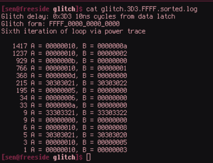
In some applications of fault injection, this degree of ambiguity is acceptable, such as breaking infinite loops, as sometimes seen in secure boot bypass techniques. However, for more complex attacks where specific operations need to be disrupted in the correct manner, higher specificity is required, necessitating a finer understanding.
While this does not provide a definitive answer for the observed behavior, the conjecture far exceeds the level of information obtained through power tracking analysis and similar techniques.