1. System Introduction
1. Signal Generator Introduction
A signal generator is an electronic device capable of producing standard or specific electrical signals, widely used in electronic testing, equipment calibration, and educational experiments. The signal generator implemented in this design can generate four basic waveforms:
-
Square Wave: A rectangular wave alternating between high and low levels
-
Sine Wave: A smooth periodic oscillating waveform
-
Triangle Wave: A waveform with linear rise and fall
-
Sawtooth Wave: A waveform that rises linearly and then quickly falls (or vice versa)
2. Detailed Explanation of MCP4921 Chip
The MCP4921 is a 12-bit Digital-to-Analog Converter (DAC) from Microchip, with the following main features:
-
12-bit Resolution (4096 output levels)
-
SPI Interface Communication (up to 20MHz)
-
Operating Voltage 2.7V-5.5V
-
Output Setup Time 4.5μs
-
Selectable 1x or 2x Output Gain
-
Low Power Design (typical 0.5mA)
Register configuration format:
Bit 15: 0 = Write to DAC, 1 = Ignored
Bit 14: BUF: VREF input buffer control
Bit 13: GA: Output gain selection (1=2x, 0=1x)
Bit 12: SHDN: Output shutdown control (1=active output, 0=high impedance)
Bit 11-0: DAC data bits (D11-D0)
3. Detailed Explanation of MCP1525 Chip
The MCP1525 is a high-precision 2.5V voltage reference source:
-
Output Voltage: 2.5V ±0.4%
-
Output Current: Maximum 15mA
-
Temperature Coefficient: 50ppm/°C
-
Low Noise: 35μV RMS
-
Operating Voltage: 4.5V to 5.5V
2. Hardware Design
1. STM32CubeMX Configuration
-
Select STM32F103C6Tx chip
-
Configure the clock tree: Use 8MHz HSI, PLL multiplied to 72MHz
-
SPI1 Configuration:
-
Full-duplex master mode
-
Hardware NSS disabled
-
Clock polarity low, phase 1 edge
-
Data width 8 bits
-
MSB first
-
Prescaler 32 (SPI clock approximately 2.25MHz)
GPIO Configuration:
-
PB0-PB3: Input mode, pull-up
-
PA4: GPIO output (MCP4921 CS)
-
PA5: SPI1 SCK
-
PA7: SPI1 MOSI
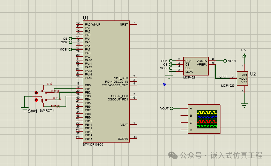
2. Proteus Circuit Design
Main components:
-
STM32F103C6
-
MCP4921
-
MCP1525
-
Single Pole Multi-Throw Switch SW-ROT-4
-
Virtual Oscilloscope
Connection method:
-
MCP1525 output 2.5V connected to MCP4921 VREF
-
MCP4921 VDD connected to 3.3V
-
CS connected to PA4, SCK connected to PA5, SDI connected to PA7
-
LDAC grounded (continuous update)
-
PB0-PB3 connected to four push-button switches
3. Software Implementation
int main(void)
{
/* USER CODE BEGIN 1 */
/* USER CODE END 1 */
/* MCU Configuration——————————————————–*/
/* Reset of all peripherals, Initializes the Flash interface and the Systick. */
HAL_Init();
/* USER CODE BEGIN Init */
/* USER CODE END Init */
/* Configure the system clock */
SystemClock_Config();
/* USER CODE BEGIN SysInit */
/* USER CODE END SysInit */
/* Initialize all configured peripherals */
MX_GPIO_Init();
MX_SPI1_Init();
MX_USART1_UART_Init();
/* USER CODE BEGIN 2 */
// Initialize the MCP492X
MCP4921_Init(&hdac, MCP4921, &hspi1, GPIOA, GPIO_PIN_4, NULL, 0);
int analogValue;
/* USER CODE END 2 */
/* Infinite loop */
/* USER CODE BEGIN WHILE */
while (1)
{
/* USER CODE END WHILE */
/* USER CODE BEGIN 3 */
if(HAL_GPIO_ReadPin(GPIOB,GPIO_PIN_0)==0)
{
MCP4921_Output(&hdac, 0);
HAL_Delay(100);
MCP4921_Output(&hdac, 4095);
HAL_Delay(100);
}
if(HAL_GPIO_ReadPin(GPIOB,GPIO_PIN_1)==0)
{
for(i=0; i<256; i++)
{
MCP4921_Output(&hdac,sin_data[i]);
HAL_Delay(1); //
}
}
if(HAL_GPIO_ReadPin(GPIOB,GPIO_PIN_2)==0)
{
for(i=0; i<256; i++)
{
MCP4921_Output(&hdac,Triangle[i]);
HAL_Delay(1); //
}
}
if(HAL_GPIO_ReadPin(GPIOB,GPIO_PIN_3)==0)
{
for(i=0; i<256; i++)
{
MCP4921_Output(&hdac,Sawtooth[i]);
HAL_Delay(1); //
}
}
}
/* USER CODE END 3 */
}
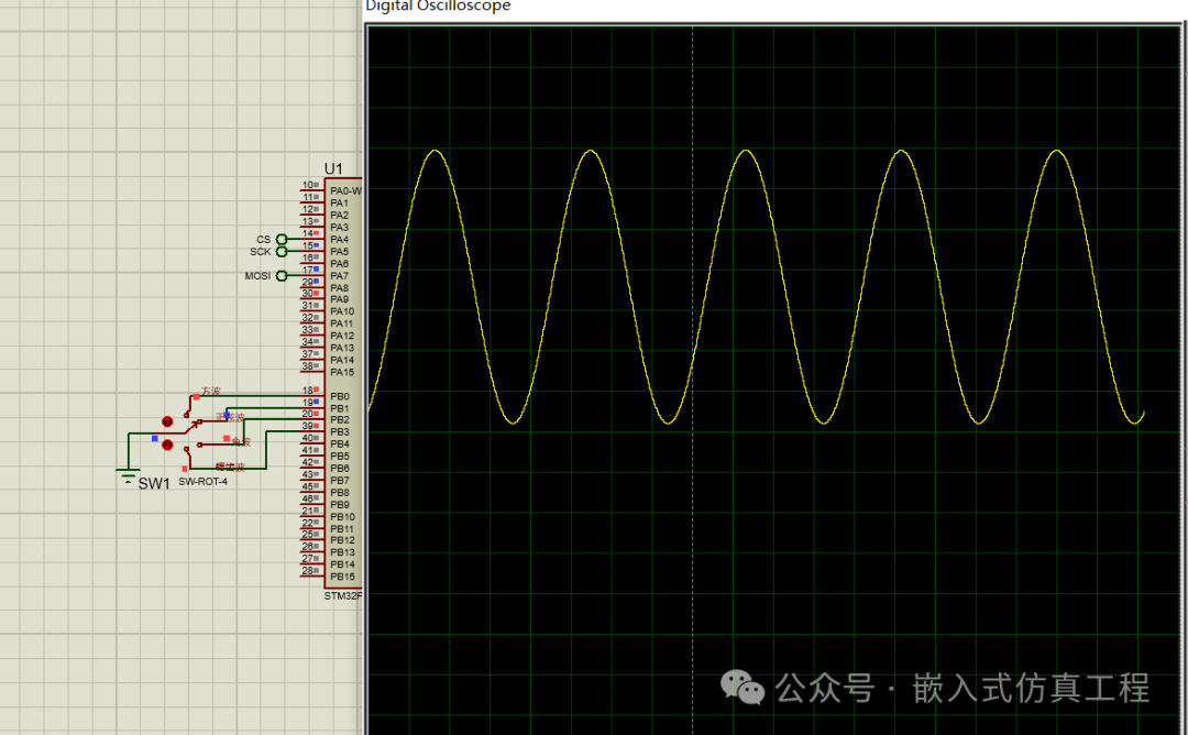
4. Proteus Simulation Instructions
-
Create a new project and add the following components:
-
STM32F103C6
-
MCP4921
-
MCP1525
-
Single Pole Multi-Throw Switch SW-ROT-4
-
Virtual Oscilloscope
Connect the circuit:
-
MCP1525 VOUT connected to MCP4921 VREF
-
MCP4921 VDD connected to 3.3V, VSS grounded
-
SPI interface connected as per previous configuration
-
MCP4921 VOUT connected to oscilloscope channel A
Load the compiled HEX file to STM32
Run the simulation, switch waveform types by clicking the up and down arrow buttons on the single pole multi-throw switch, and observe the output waveform on the oscilloscope
5. Performance Optimization Suggestions
-
Use DMA transfer to improve SPI communication efficiency
-
Pre-calculate waveform tables stored in ROM to reduce real-time computation
-
Add frequency adjustment functionality
-
Implement waveform amplitude adjustment
-
Add LCD to display current waveform type and parameters
Through the above design, a simple signal generator based on STM32 and MCP4921 has been implemented, capable of generating four basic waveforms, and the system functionality has been verified through Proteus simulation.