
1. Industry Trends: From 2D to 3D DRAM, Establishing the Trend of Storage-Computing Integration
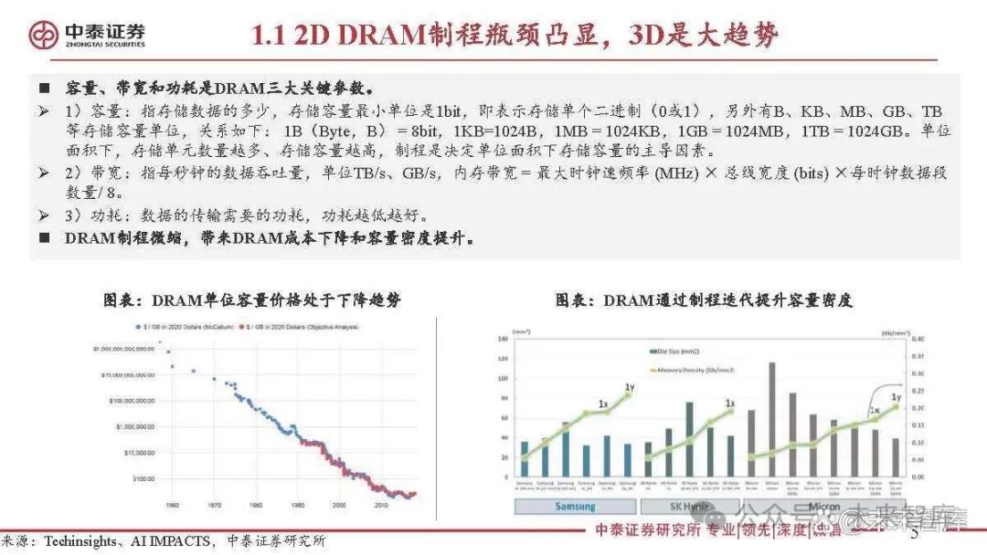
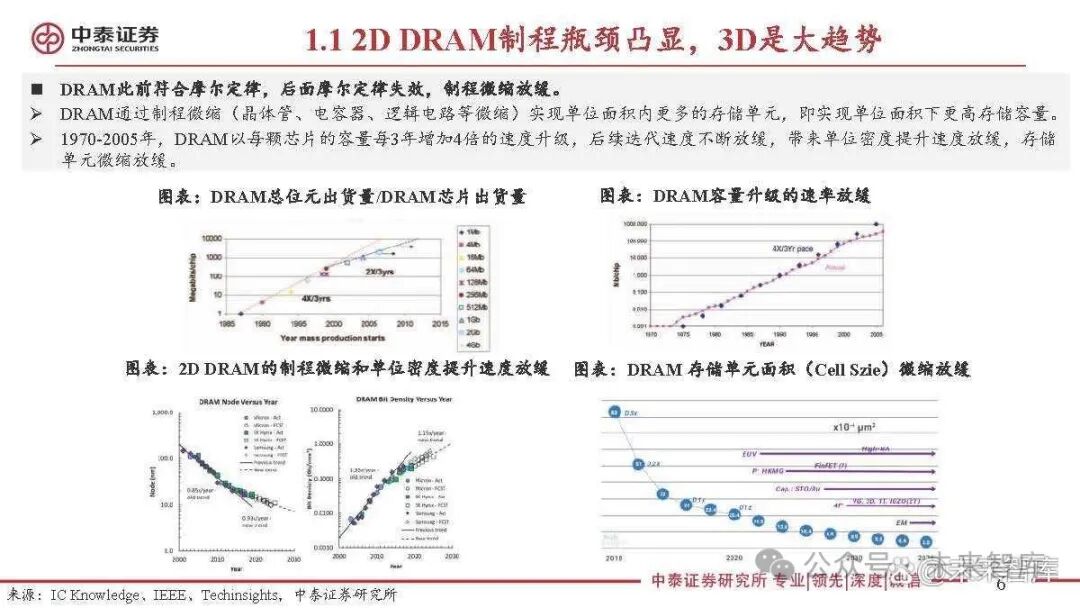
The bottleneck of 2D DRAM processes is becoming apparent; 3D is the major trend.
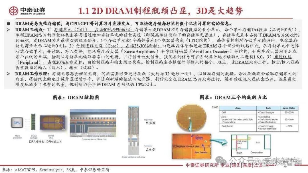
DRAM is a volatile memory that interacts directly with computing chips such as CPUs and GPUs, allowing for rapid storage of the information needed for billions of calculations executed per second.
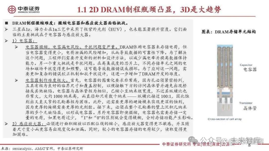
Three components of DRAM: 1) Storage Cells (Cell), occupying 50%-55% of the area: The storage cell is the smallest unit of data storage in a DRAM chip, with each cell storing 1 bit of data (binary 0 or 1). The capacity expansion of a single DRAM chip is mainly achieved by increasing the number of storage cells (i.e., increasing the density of storage cells per unit area). Storage cells occupy about 50-55% of the area of a DRAM chip and are the core component of DRAM chips. A storage cell consists of 1 transistor and 1 capacitor (1T1C structure), where the transistor controls access to the storage cell, and the capacitor stores charge to represent binary 0 or 1. 2) Peripheral Logic Circuits (Core), occupying 25-30% of the area: Composed of logic transistors and lines connecting various parts of the DRAM, selecting the required storage cells and reading/writing data, including structures such as Sense Amplifiers and Word Line Decoders. For example, sense amplifiers are attached at the end of each bit line to detect very small charges read from storage cells and amplify the signal, allowing the amplified signal to be read elsewhere in the system as binary 1 or 0. 3) Peripheral Lines (Peripheral), occupying about 20% of the area: Composed of control lines and output lines. Control lines mainly operate the DRAM internally based on external input commands and addresses. Input/output lines are responsible for data input (writing) and output (reading).
The working principle of DRAM: Storage capacitors leak charge, so they need to be refreshed frequently (approximately every 32 milliseconds) to maintain stored data. Each refresh reads the contents of the storage cell, raises the voltage on the bit line to an ideal level, and allows the refreshed value to flow back to the capacitor. The refresh operation is entirely conducted within the DRAM chip, with no data flowing in or out of the chip. Although this minimizes wasted power, refreshing still accounts for over 10% of the total power consumption of DRAM.
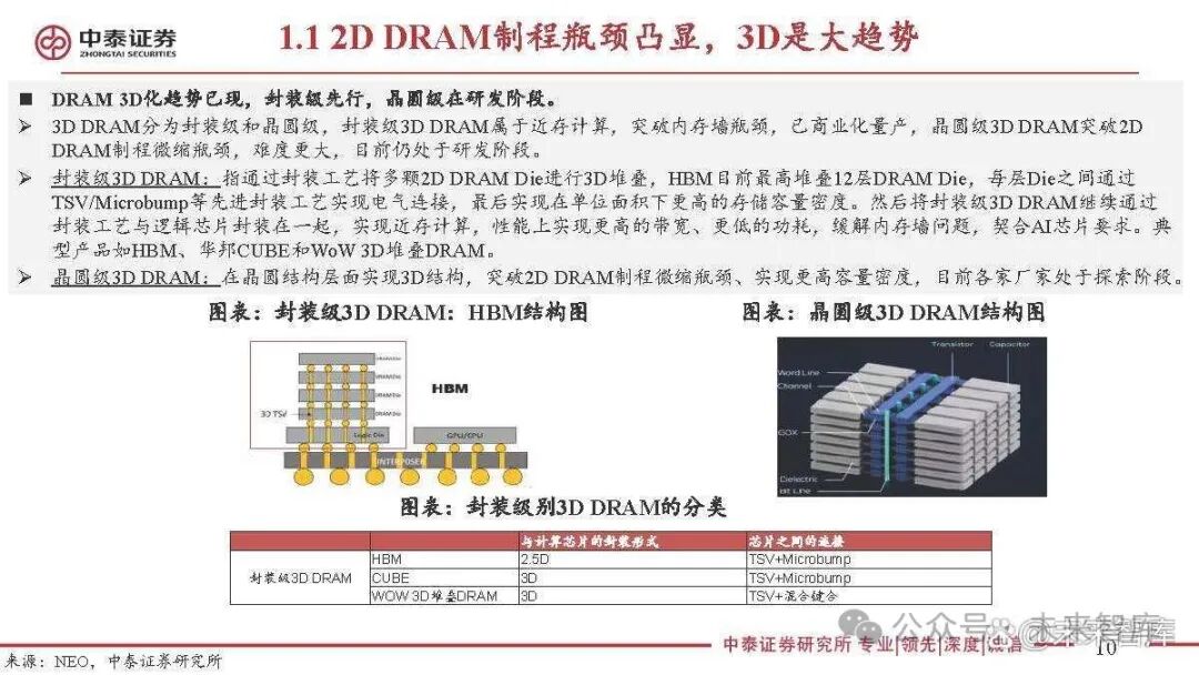
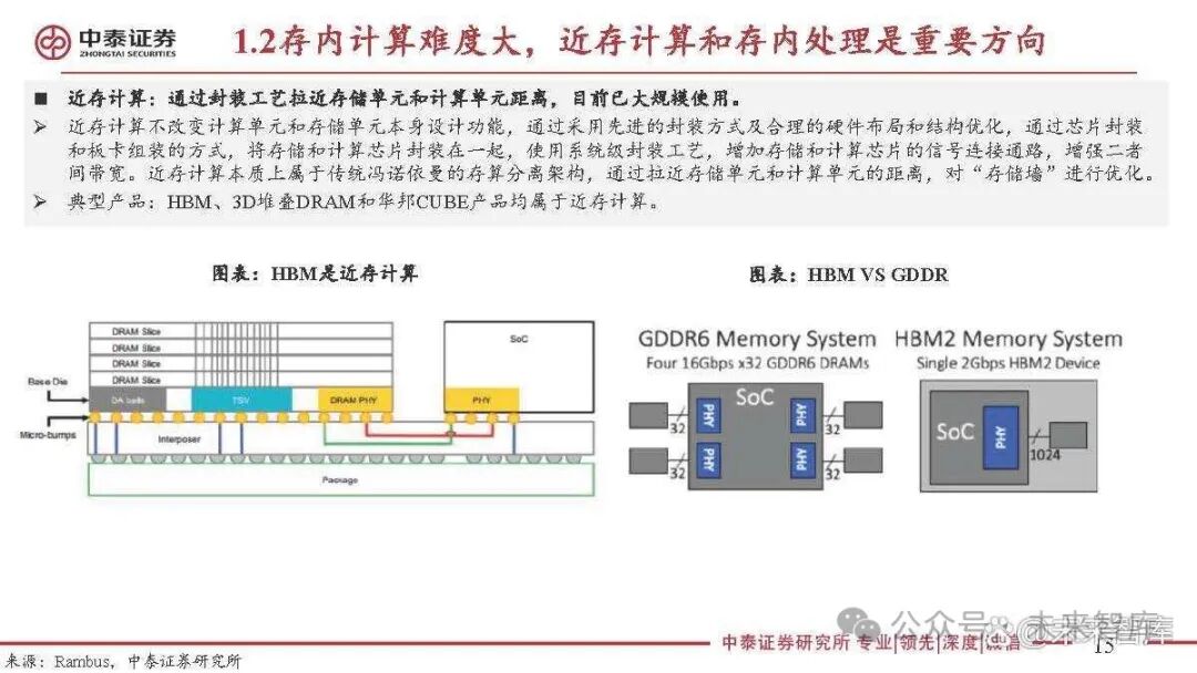
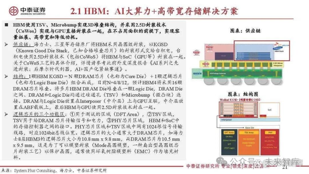
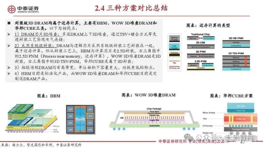
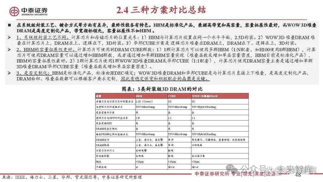
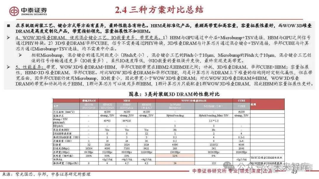
The trend of 3D DRAM is emerging, with packaging-level advancements leading the way, while wafer-level developments are still in the research phase. 3D DRAM is divided into packaging-level and wafer-level. Packaging-level 3D DRAM belongs to near-memory computing, breaking through the memory wall bottleneck and has been commercially mass-produced. Wafer-level 3D DRAM aims to overcome the scaling bottlenecks of 2D DRAM processes, which is more challenging and is currently still in the research phase. Packaging-level 3D DRAM: This refers to the 3D stacking of multiple 2D DRAM dies through packaging technology. HBM currently stacks up to 12 layers of DRAM dies, with electrical connections between layers achieved through advanced packaging technologies such as TSV/Microbump, ultimately achieving higher storage capacity density per unit area. The packaging-level 3D DRAM is then further packaged together with logic chips to achieve near-memory computing, resulting in higher bandwidth, lower power consumption, and alleviating the memory wall issue, aligning with the requirements of AI chips. Typical products include HBM, Winbond CUBE, and WoW 3D stacked DRAM. Wafer-level 3D DRAM: This aims to achieve a 3D structure at the wafer level, breaking through the scaling bottlenecks of 2D DRAM processes to achieve higher capacity density, with various manufacturers currently exploring this stage.
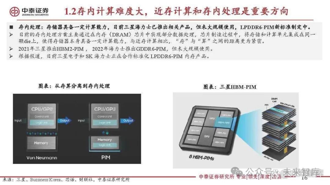
In-memory computing is challenging; near-memory computing and in-memory processing are important directions.
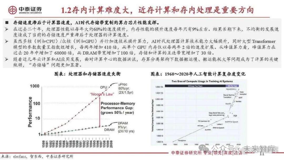
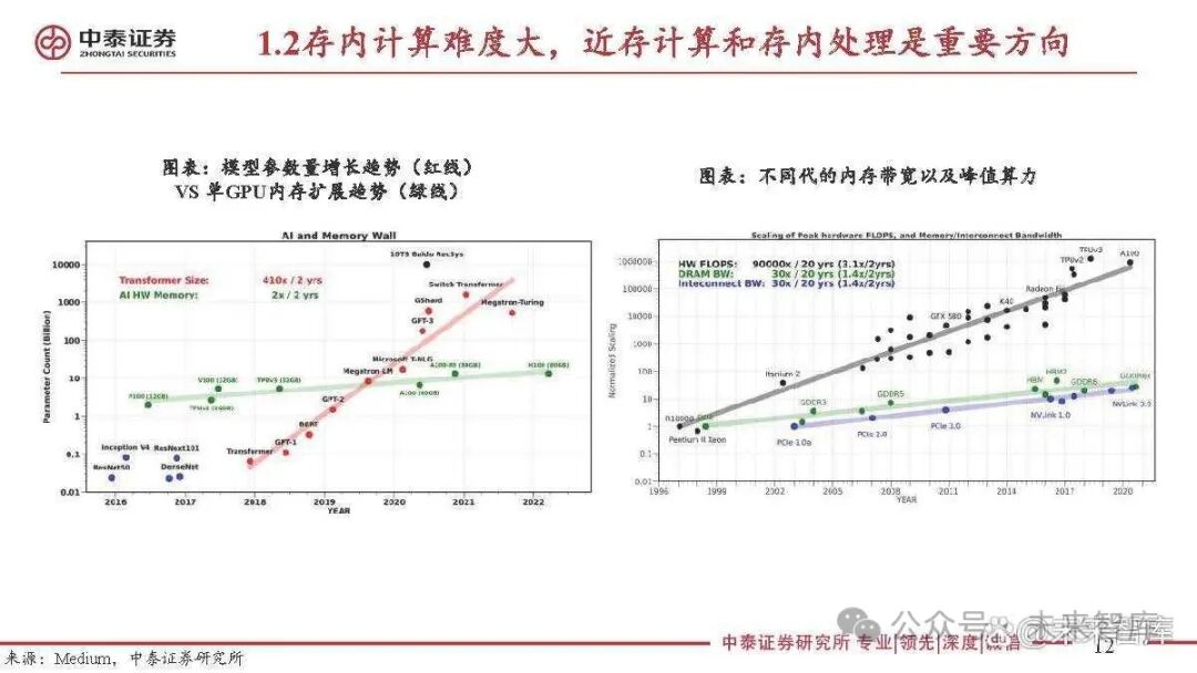
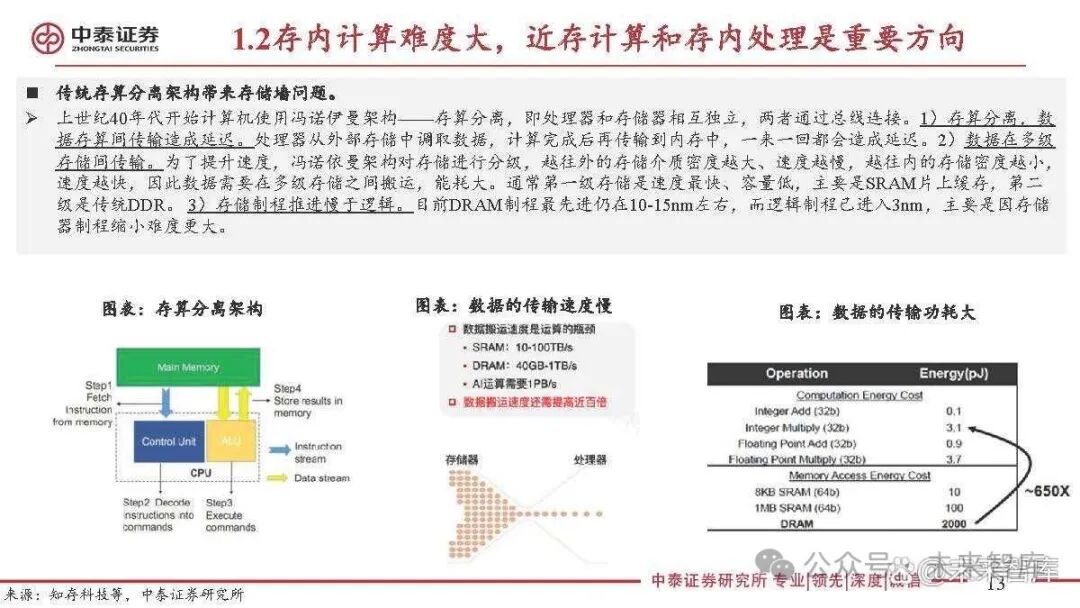
The speed of storage lags behind that of processors, and in the AI era, storage bandwidth constrains the performance of computing chips. Over the past two decades, processor performance has improved at a rate of about 60% per year, while memory performance has only improved by about 9% per year. As a result, the long-term imbalance in development speeds has led to a significant lag in storage speed compared to processor computing speed. Although multi-core (e.g., CPU) and many-core (e.g., GPU) parallel acceleration technologies enhance computing power, the computational capabilities of processors have significantly improved in the AI era, while the number of parameters in large Transformer models has increased exponentially, growing 410 times every two years, whereas the memory of a single GPU has only expanded at a rate of 2 times every two years. From the perspective of peak computing power, peak computing power has increased 60,000 times over the past 20 years, while DRAM bandwidth has only increased 100 times, and the interconnect bandwidth between storage and computing has increased 30 times. With the recent development of cloud computing and AI applications, the issues of slow data transport and high transport energy consumption under a storage-computing separation architecture have become critical bottlenecks in computing, making the “memory wall” problem even more pronounced.
2. Packaging-Level 3D DRAM: Near-Memory Computing, High Bandwidth, Low Power Consumption to Meet AI Scene Requirements
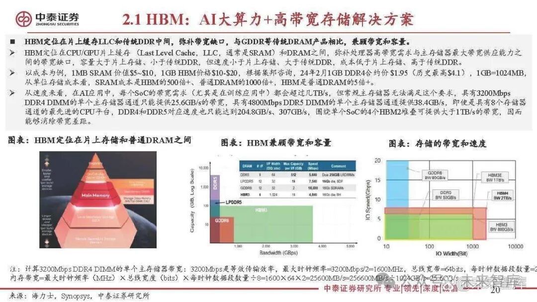
HBM: AI High Computing Power + High Bandwidth Storage Solution
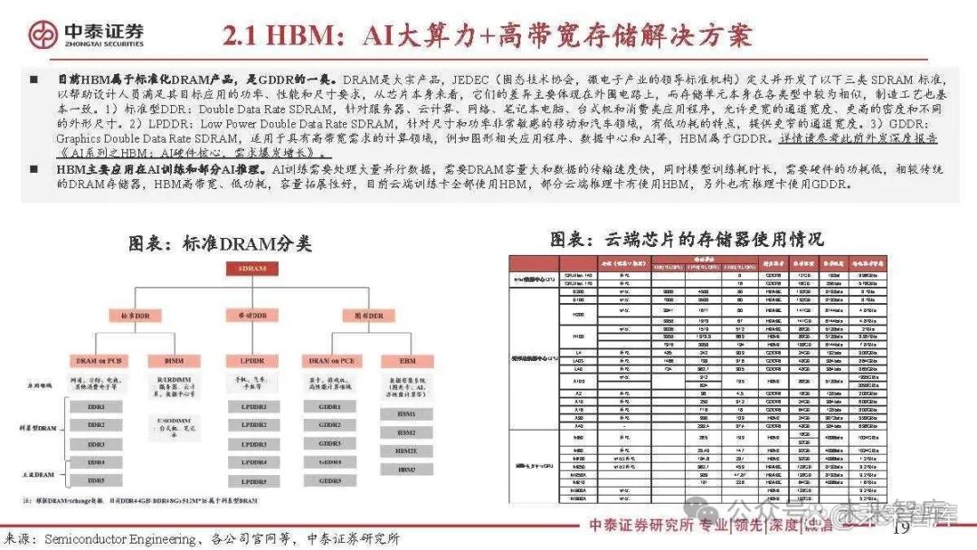
Currently, HBM is a standardized DRAM product, a type of GDDR. DRAM is a bulk product, and JEDEC (the Solid State Technology Association, the leading standards organization in the microelectronics industry) has defined and developed the following three types of SDRAM standards to help designers meet their power, performance, and size requirements for target applications. From the perspective of the chip itself, their differences mainly lie in the peripheral circuits, while the storage cells themselves are quite similar across types, and the manufacturing processes are fundamentally consistent. 1) Standard DDR: Double Data Rate SDRAM, aimed at servers, cloud computing, networking, laptops, desktops, and consumer applications, allowing for wider channel widths, higher densities, and different form factors. 2) LPDDR: Low Power Double Data Rate SDRAM, aimed at mobile and automotive fields that are very sensitive to size and power, characterized by low power consumption and providing narrower channel widths. 3) GDDR: Graphics Double Data Rate SDRAM, suitable for computing fields with high bandwidth requirements, such as graphics-related applications, data centers, and AI, with HBM belonging to GDDR. For more details, please refer to the previous in-depth report “HBM: The Core of AI Hardware, Demand Explosion Growth”.
HBM is mainly used in AI training and some AI inference. AI training requires processing a large amount of parallel data, necessitating large DRAM capacity and fast data transfer speeds, while model training takes a long time and requires low hardware power consumption. Compared to traditional DRAM memory, HBM offers high bandwidth, low power consumption, and good capacity scalability. Currently, all cloud training cards use HBM, and some cloud inference cards also use HBM, while others use GDDR for inference cards.
WOW 3D Stacked DRAM: AI Low Computing Power + Ultra High Bandwidth Storage Solution
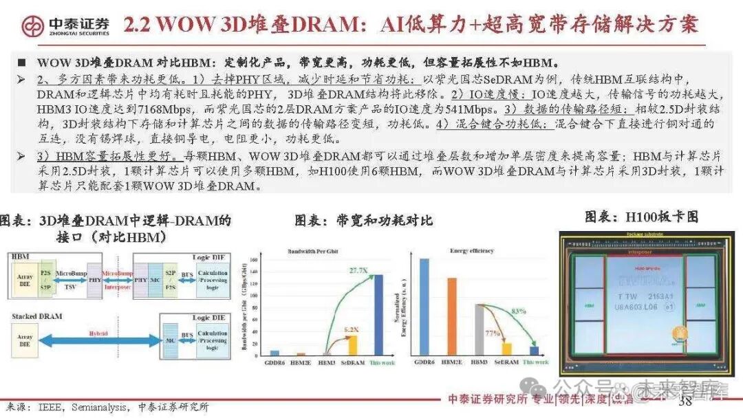
WOW 3D stacked DRAM is a 3D structure with logic chips, belonging to near-memory computing. Structure: It belongs to near-memory computing, where DRAM and logic chips are packaged together using 3D stacking technology, stacking multiple layers of DRAM chips on a single logic chip, where the logic chip refers to computing chips such as GPU, CPU, NPU, etc. The purple Logic Die in the right image represents this, while the DRAM chip image shows only one layer, but multiple layers can actually be stacked. Technology: It uses TSV (Through-Silicon Via) technology and Wafer on Wafer hybrid bonding technology to achieve electrical connections between multiple layers of chips. Performance characteristics: Taking the WOW 3D stacked DRAM product SeDRAM from Unisoc as an example, the pitch between vias reaches below 10μm, while HBM’s pitch is currently in the tens of micrometers, thus WOW 3D stacked DRAM has higher bandwidth and lower power consumption, and is a customized product with general capacity scalability.
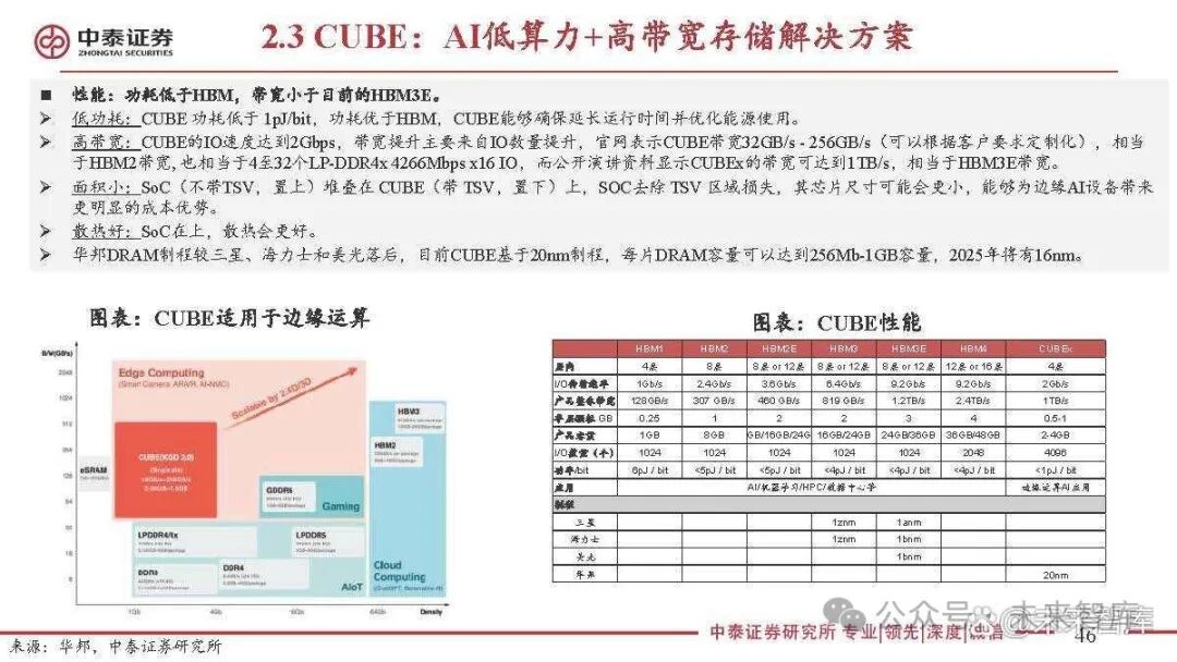
CUBE: AI Low Computing Power + High Bandwidth Storage Solution
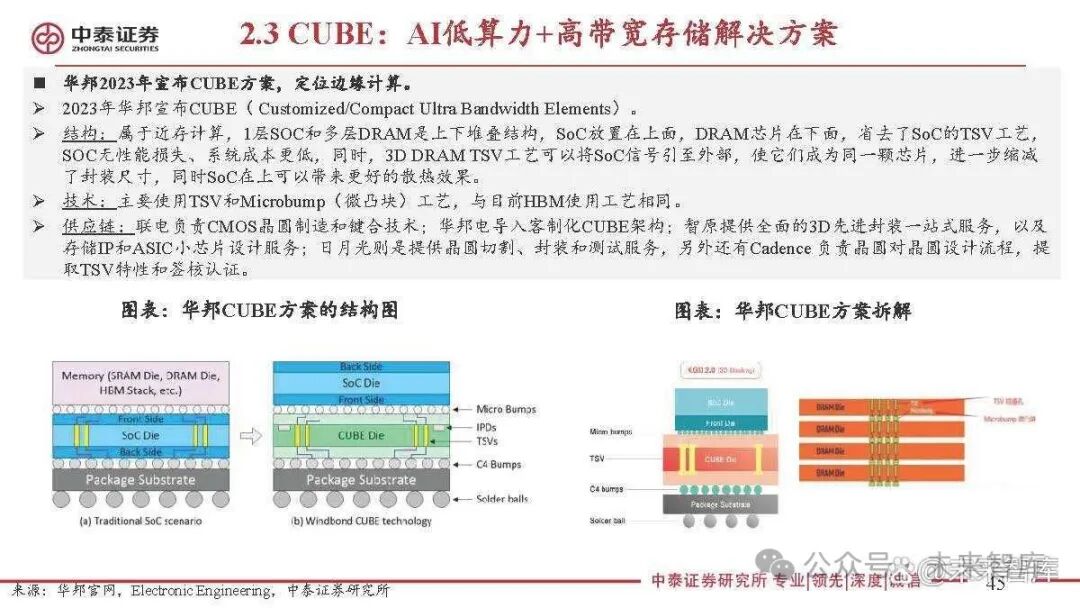
In 2023, Winbond announced the CUBE solution, targeting edge computing. In 2023, Winbond announced CUBE (Customized/Compact Ultra Bandwidth Elements). Structure: It belongs to near-memory computing, with one layer of SoC and multiple layers of DRAM stacked vertically, with the SoC placed on top and the DRAM chips below, eliminating the TSV process for the SoC, resulting in no performance loss for the SoC and lower system costs. Additionally, the 3D DRAM TSV process can route SoC signals to the outside, making them part of the same chip, further reducing packaging size, while the SoC on top can provide better heat dissipation. Technology: It mainly uses TSV and Microbump technology, similar to the current HBM manufacturing process. Supply chain: UMC is responsible for CMOS wafer manufacturing and bonding technology; Winbond introduces the customized CUBE architecture; Zhi Yuan provides comprehensive 3D advanced packaging one-stop services, as well as storage IP and ASIC small chip design services; ASE provides wafer cutting, packaging, and testing services, and Cadence is responsible for the wafer-to-wafer design process, extracting TSV characteristics and certification.
3. Wafer-Level 3D DRAM: Breaking Through Process Bottlenecks, Currently Exploring Multiple Solutions
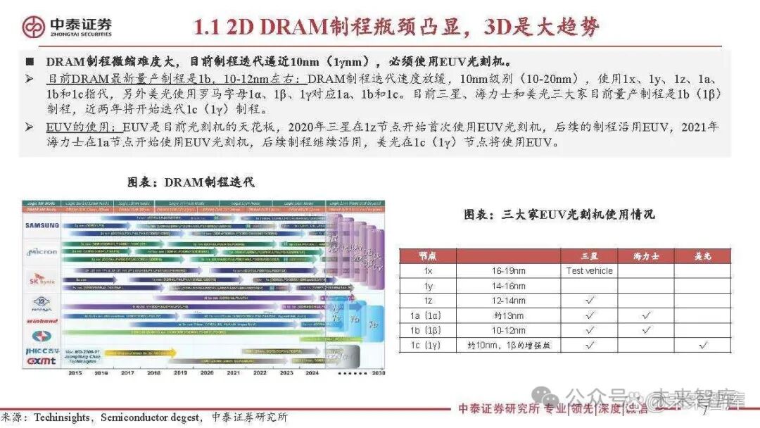
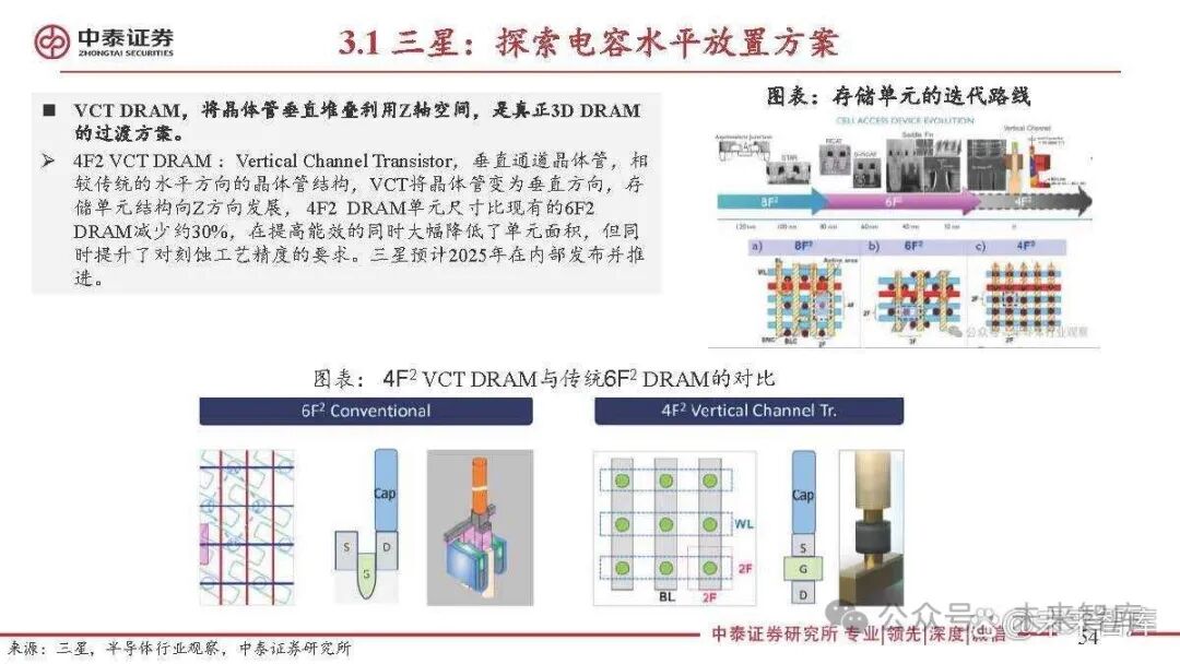
Samsung & SK Hynix: Exploring Capacitor Horizontal Placement Solutions
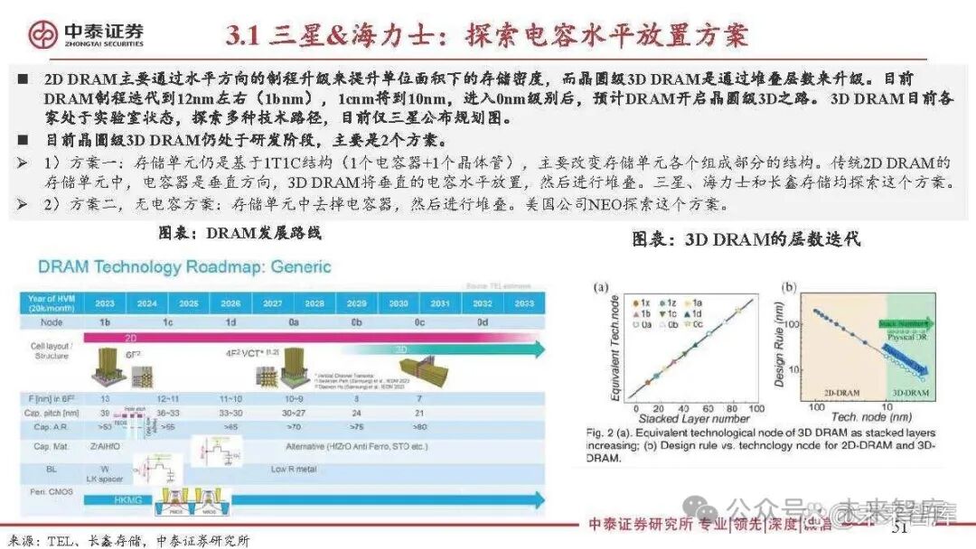
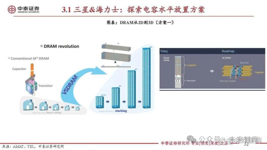
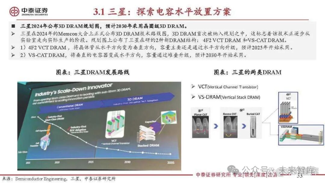
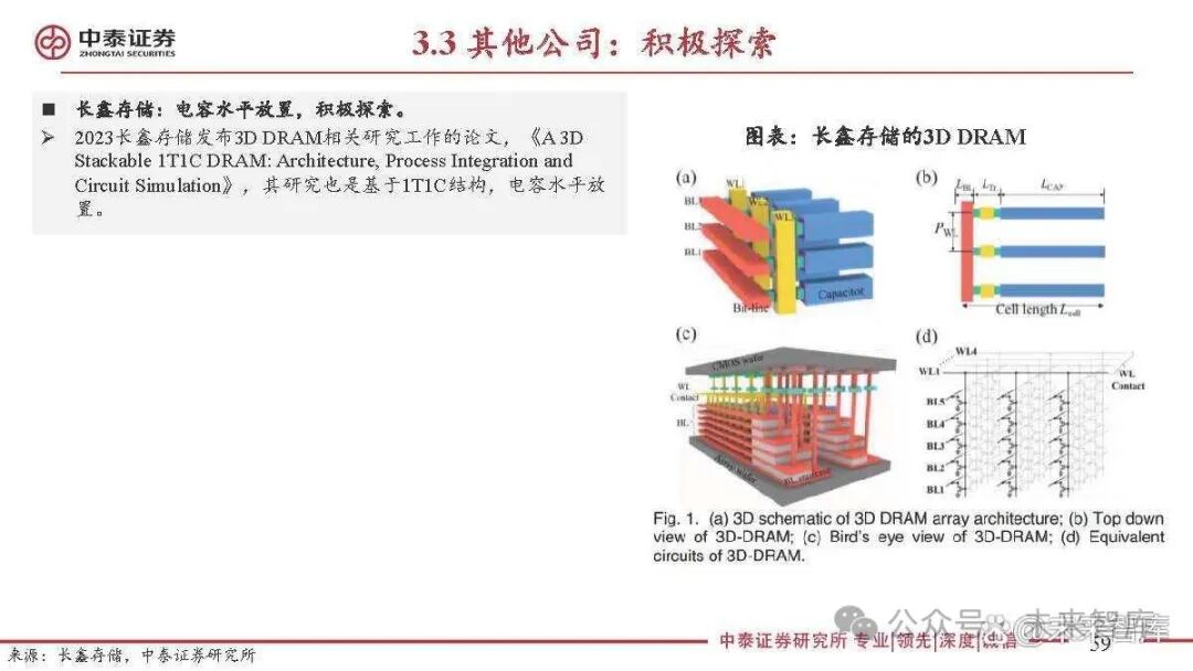
2D DRAM mainly enhances storage density per unit area through horizontal process upgrades, while wafer-level 3D DRAM upgrades through the number of stacked layers. Currently, DRAM processes have iterated to around 12nm (1bnm), and 1cnm will reach 10nm. Once entering the 0nm level, it is expected that DRAM will embark on the wafer-level 3D path. Currently, various manufacturers are in the laboratory stage, exploring multiple technical paths, with only Samsung publishing a planning diagram. Currently, wafer-level 3D DRAM is still in the research phase, with two main solutions. 1) Solution one: The storage cell is still based on the 1T1C structure (1 capacitor + 1 transistor), mainly changing the structure of each component of the storage cell. In traditional 2D DRAM, the capacitor is oriented vertically, while 3D DRAM will place the vertical capacitor horizontally and then stack it. Samsung, SK Hynix, and Changxin Memory are exploring this solution. 2) Solution two, capacitor-less solution: The storage cell removes the capacitor and then stacks it. The American company NEO is exploring this solution.
NEO Company: Exploring Capacitor-Less Solutions
NEO: Adopts a capacitor-less solution. In 2023, the American storage company NEO announced the 3D-X DRAM technology, which features a capacitor-less floating gate (FBC) technology-based quasi-3D NAND DRAM cell array structure. This FBC floating gate technology uses one transistor and zero capacitors to store data as charge. NEO Semiconductor claims it can be manufactured using current 3D NAND-like processes and only requires an additional layer of photomask to define bit line holes and form vertical structures within the holes, providing a high-speed, high-density, low-cost, and high-yield manufacturing solution. According to NEO’s estimates, the 3D X-DRAM technology can achieve a density of 230 layers of 128 Gb, which is 8 times the current DRAM density. NEO proposes a goal of achieving an 8-fold capacity increase every 10 years, aiming for a capacity of 1Tb between 2030 and 2035, which is a 64-fold increase over the current DRAM core capacity, meeting the growing demand for high-performance and large-capacity storage semiconductors for AI applications like ChatGPT.
Report Excerpt:
 Source: Future Think Tank