1. Introduction
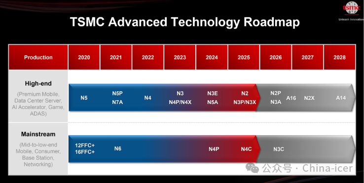
In the semiconductor industry, every breakthrough in process technology is akin to a technological revolution, redefining the boundaries of chip performance and injecting powerful vitality into the fields of intelligent electronic devices and high-performance computing. On April 24, 2025, TSMC officially announced at the 2025 Technology Symposium in the United States that its A14 process will enter mass production in 2028. This technological breakthrough marks the official entry of the global semiconductor industry into the 1.4nm era, profoundly impacting the HPC and AI fields, while also presenting significant challenges and opportunities for the mainland computing chip and automotive chip industries.
2. Core Technologies and Performance Improvements of TSMC A14 Process
(1) Transistor Technology Upgrade: From FinFET to GAAFET
The TSMC A14 process adopts second-generation GAAFET transistor technology, which has significant advantages in performance and power consumption compared to traditional FinFET transistors. GAAFET can better control leakage, improve the switching speed and performance of transistors, and the nanosheet design allows for more precise current control, achieving higher performance and lower power consumption.
(2) Multidimensional Impact of Performance Improvement
• Speed and Power Consumption Optimization: Compared to the N2 process, which is set to enter mass production later in 2025, the A14 process can provide up to a 15% speed increase at the same power consumption or reduce power consumption by up to 30% at the same speed.
• Logic Density Improvement: Logic density has increased by over 20%, meaning that more transistors can be integrated on the same chip area, enabling more complex functions and performance enhancements.
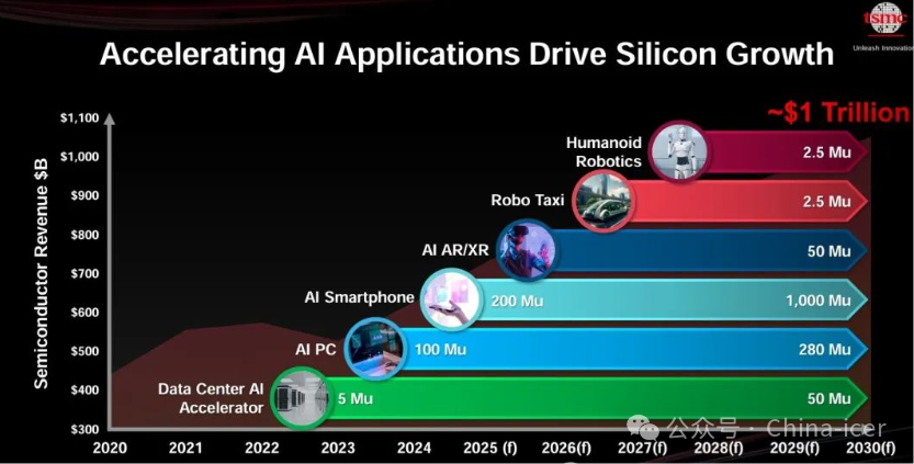
• Impact on HPC and AI: In the HPC and AI fields, the high performance and low power characteristics of the A14 process make it an ideal choice. For example, deep learning (DL) and machine learning (ML) in AI require substantial computational resources, and the A14 process can significantly enhance computational efficiency.
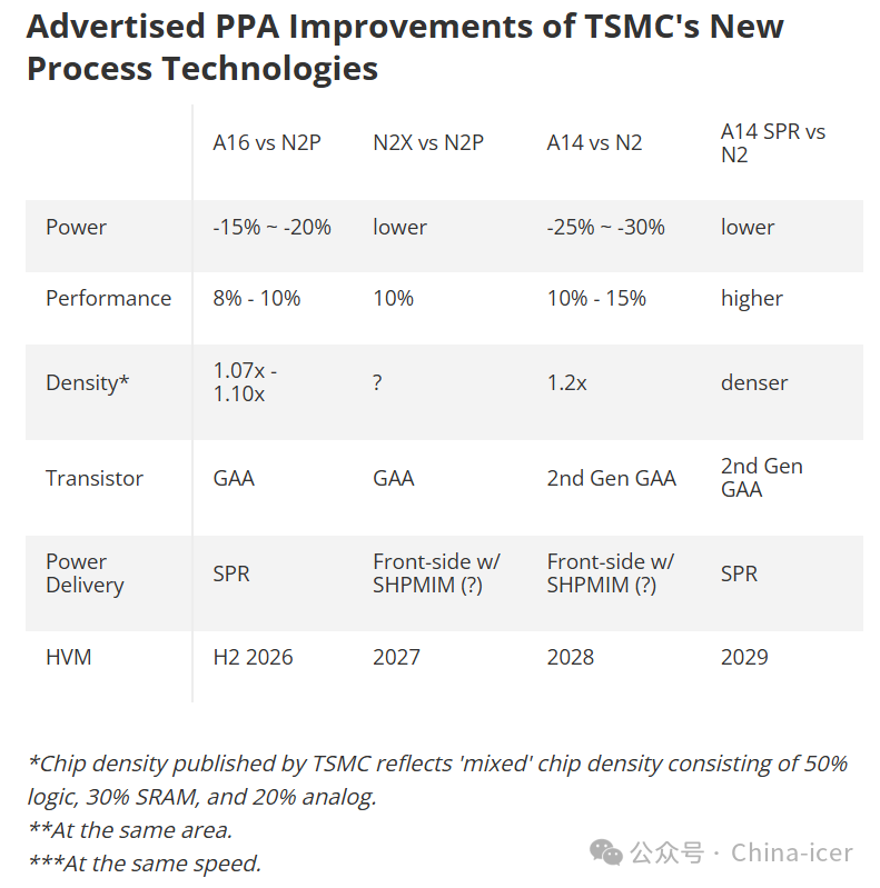
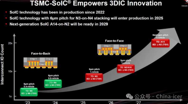
Unlike the A16 (similar to N2 and N2P), the A14 lacks a Super Power Rail (SPR) backside power delivery network (BSPDN), allowing this technology to target applications that cannot benefit from BSPDN, as it incurs additional costs.
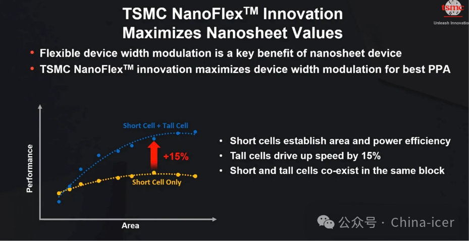
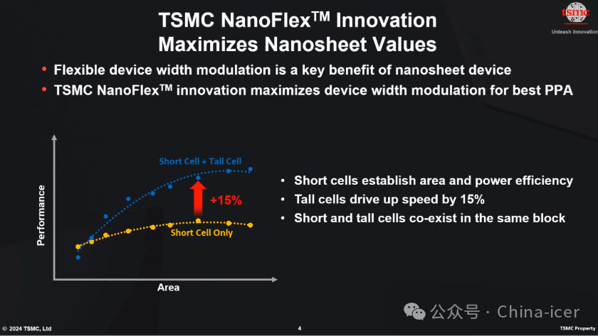
This technology also employs our NanoFlex Pro technology, which is essentially a Design Technology Co-Optimization (DTCO) that allows designers to create products in a very flexible manner, helping them achieve optimal power performance advantages.
3. Impact of TSMC A14 Process on Mainland Computing Chips
(1) Technical and Market Aspects
• Technical Gaps and Challenges: The mainland still faces technical bottlenecks in high-end processes. For instance, U.S. export controls on advanced EDA tools and process equipment have made breakthroughs in processes below 7nm quite challenging.
• Opportunities for Domestic Substitution: Despite facing technical challenges, external pressures have accelerated the domestic substitution process for mainland computing chips. Companies like Huawei, Haiguang, and Cambricon are making strides in the domestic substitution market, gradually improving their products in terms of performance and power optimization.
(2) Data Aspects
• Growing Demand for Computing Power: According to the “China Intelligent Computing Market Scale Research Report” published by Kezhi Consulting, the supply scale of AIDC computing power in China is expected to maintain a rapid growth rate of nearly 40% from 2024 to 2028.
• Explosive Demand on the Inference Side: The proportion of inference-side demand is expected to grow from the current 65% to 72% by 2027.
(3) Industry and Competitive Landscape
• Intensifying Global Competition: The launch of the TSMC A14 process will intensify competition in the global computing chip market. Mainland computing chip manufacturers need to accelerate their pace in technological innovation and market positioning to cope with competitive pressures from TSMC, Intel, and Samsung.
• Response Strategies of Domestic Chip Manufacturers: Mainland chip companies are enhancing their competitiveness through technological innovation and ecosystem development. For example, DeepSeek has reduced reliance on high-performance GPU computing power through algorithmic innovation, enabling domestic chips to achieve high-performance operation in inference scenarios.
4. Impact of TSMC A14 Process on Mainland Automotive Chips
(1) Technical and Market Aspects
• Growing Demand for Automotive Chips: With the development of automotive intelligence and electrification, the demand for automotive chips continues to grow. Automotive chips have extremely high reliability and safety requirements, and the high logic density and low power characteristics of the TSMC A14 process make it potentially valuable in the automotive chip field.
• Current Status of Mainland Automotive Chips: The mainland has made certain progress in the automotive chip field, but still relies on imports for high-end automotive chips. For instance, in areas like automotive MCUs and power devices, mainland companies are gradually squeezing the market share of American manufacturers through cost advantages and localized support.
• Acceleration of Domestic Substitution: The tariff war and external pressures have prompted the mainland to accelerate the domestic substitution of automotive chips. For example, in 2024, MediaTek’s market share in the flagship smartphone chip market in mainland China has approached 40%, indicating…
(2) Data Aspects
• Market Share: In 2024, MediaTek’s market share in the flagship smartphone chip market in mainland China has approached 40%, demonstrating the competitiveness of domestic chips in the mid-to-low-end market.
• Tariff Impact: Starting in 2025, U.S. tariffs on semiconductor exports to mainland China will increase from 25% to 50%, further impacting the ecosystem of China’s semiconductor industry.
(3) Industry and Competitive Landscape
• Global Competitive Landscape: The launch of the TSMC A14 process will intensify competition in the global automotive chip market. Mainland automotive chip manufacturers need to accelerate their pace in technological innovation and market positioning to cope with competitive pressures from TSMC, Intel, and Samsung.
• Response Strategies of Domestic Automotive Chip Manufacturers: Mainland automotive chip companies are enhancing their competitiveness through technological innovation and ecosystem development. For instance, Ascend, Mthreads, and MetaX are also accelerating the adaptation of DeepSeek technology to enhance the performance and reliability of automotive chips.
5. Other Technical Details of TSMC A14 Process
(1) Breakthroughs in Packaging Technology
TSMC plans to start mass production of CoWoS packaging technology with a 9.5x mask size in 2027. This technology can integrate 12 or more HBM (High Bandwidth Memory) stacks, which is crucial for data centers and AI training. HBM plays a key role in high-performance computing, providing extremely high data transfer rates and storage capacity. By increasing the number of HBM stacks, CoWoS can significantly enhance system processing efficiency and performance.
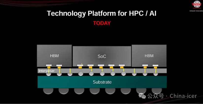
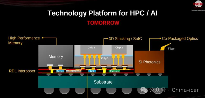
TSMC is continuing to advance its CoWoS (Chip on Wafer on Substrate) technology to meet the growing demand for more logic and HBM in AI. For instance, it plans to mass-produce a 9.5x mask size CoWoS in 2027, which will be able to integrate 12 or more HBM stacks using TSMC’s advanced logic technology.
Following the revolutionary System on Wafer (TSMC-SoW) technology released in 2024, TSMC is again introducing SoW-X based on CoWoS technology to create a wafer-sized system with 40 times the computing power of current CoWoS solutions, with SoW-X planned for mass production in 2027.
To achieve the ultimate computing power and efficiency of its logic technology, TSMC provides many solutions, including silicon photonic integration using compact general-purpose photonic engine (COUPETM) technology, bare die logic for HBM4 using N12 and N3 logic, and new integrated voltage regulators (IVR) for AI, which have 5 times the vertical power density transmission compared to independent power management chips on the circuit board.
(2) Collaborative Development of Technologies Across Multiple Fields
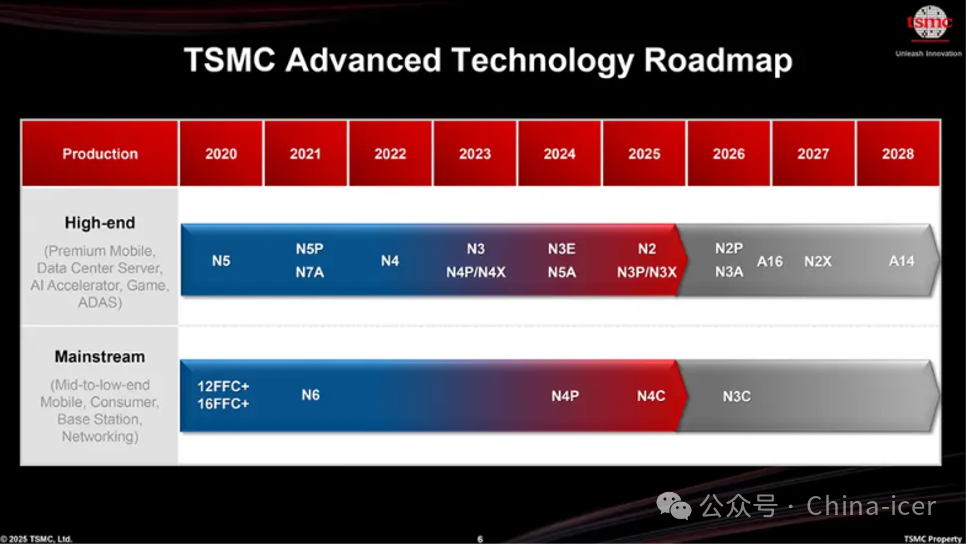
TSMC revealed that it will begin producing chips based on the performance-enhanced N3P (third-generation 3nm process technology) in the fourth quarter of 2024. N3X chips are expected to enter mass production in the second half of 2025. Compared to N3P, N3X is expected to improve maximum performance by 5% at the same power or reduce power consumption by 7% at the same frequency, supporting voltages up to 1.2V. TSMC’s technological layout across different fields reflects its precise grasp of the multi-field development trend in the semiconductor industry. Applications of N4CRF RF technology, N3A technology, and N4e process cover several important fields, including smartphones, automotive electronics, and IoT.
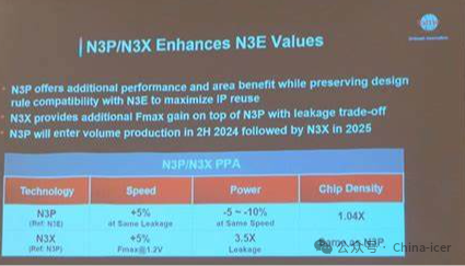
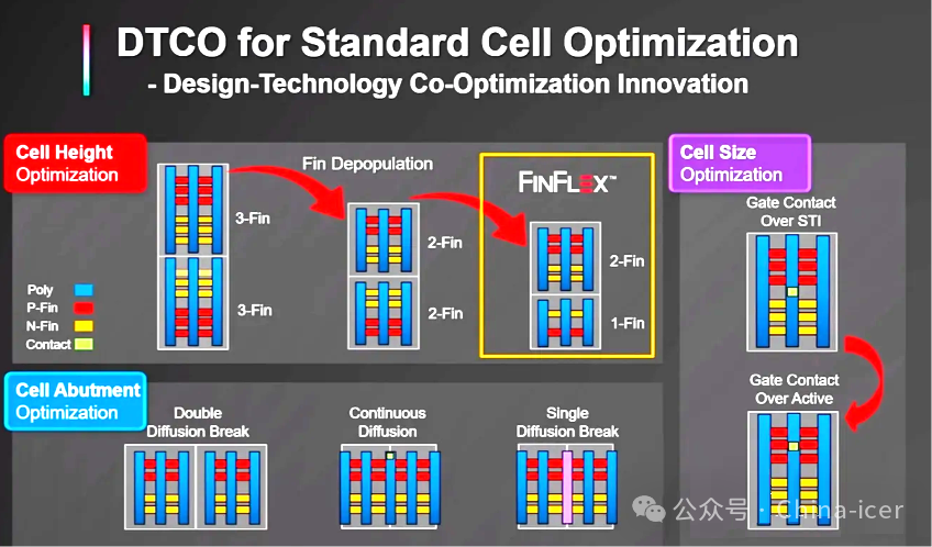
TSMC tends to provide multiple iterations of process technology within a process development kit (e.g., N5, N5P, N4, N4P, N4C). On one hand, this allows the company to use expensive equipment for as long as possible; on the other hand, it also allows its customers to reuse their IP for as long as possible. Therefore, N3P is a natural complement to the N3X production node series. 
Chip designers will adhere to a library/standard cell in SoC design, for example, a CPU core can be implemented using 3-2 fin blocks to enhance operating speed; or a 2-1 fin standard cell to reduce power consumption and area. For N3, TSMC’s FinFlex allows chip designers to mix various standard cells, enabling precise adjustments of performance, power consumption, and area. For complex structures like CPUs, this technology can be used to optimize performance.
However, FinFET cannot replace the specialization of processes, but its optimization for the N3 process is excellent, approaching the GAAFET node (providing adjustable channel widths for high performance and reduced power consumption).
6. Philosophical Reflection: The Relationship Between Technological Progress and Human Development
(1) The Essence of Technological Progress
The essence of technological progress lies in the pursuit of “better.” The transition from FinFET to GAAFET is not just a technological upgrade but also an unremitting pursuit of higher performance and lower power consumption. Behind this pursuit lies a philosophical thought: humanity’s exploration of technology is endless, and every technological breakthrough is a challenge and transcendence of existing technological limits.
(2) Interaction Between Technology and Society
Technological progress is not only the evolution of technology itself but also driven by societal needs. The development of high-performance computing (HPC) and artificial intelligence (AI) reflects modern society’s pursuit of high efficiency and low energy consumption. This demand drives technological progress, while technological progress, in turn, meets societal needs, forming a virtuous cycle.
(3) The Future of Technological Development
The future of technological development is filled with uncertainty, but one thing is certain: technological progress will continue to drive the development of human society. The competition between TSMC, Intel, and Samsung is not only a competition of technology but also a competition for the future direction of development. As Nietzsche said, “Every day that does not dance is a betrayal of life,” technological progress is a reflection of humanity’s continuous pursuit of a better life.
7. Conclusion
The launch of the TSMC A14 process marks the official entry of the global semiconductor industry into the 1.4nm era. This technological advancement presents significant challenges and opportunities for the mainland computing chip and automotive chip industries. Although the mainland still faces technical bottlenecks in high-end processes, external pressures have accelerated the domestic substitution process. Mainland computing chip and automotive chip manufacturers need to accelerate their pace in technological innovation and market positioning to cope with competitive pressures from TSMC, Intel, and Samsung. Through technological innovation and ecosystem development, mainland chip companies are expected to secure a place in the global semiconductor market and promote the high-quality development of the semiconductor industry.
—
References:
:[State-of-the-Art and Trends for Computing and Interconnect Network Solutions for HPC and AI]
:[Worldwide HPC-based Artificial Intelligence(Al)Market Forecast,2020-2026]
:[TSMC 2nm Update: N2 In 2025, N2P Loses Backside Power, and NanoFlex Brings Optimal Cells]
:[ChatGPT对GPU算力的需求测算与相关分析]
:[云从科技集团股份有限公司2022年年度报告]
:[罗博特科智能科技股份有限公司发行股份及支付现金购买资产并募集配套资金之独立财务顾问报告(修订稿)]
[智算产业发展研究报告–信科院]