Abstract
|
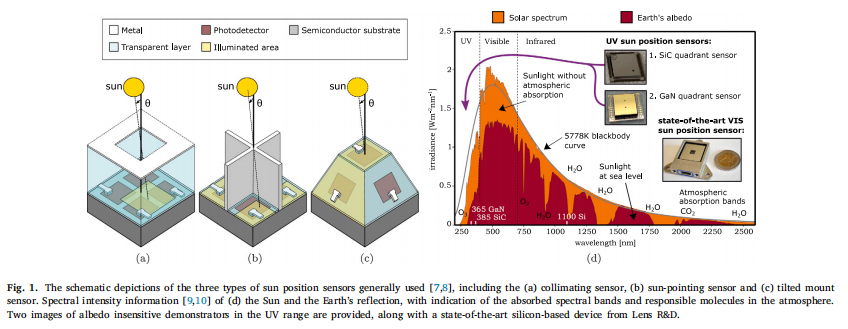
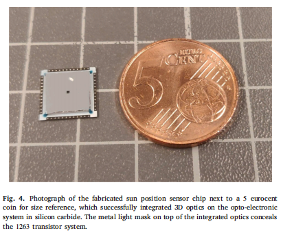
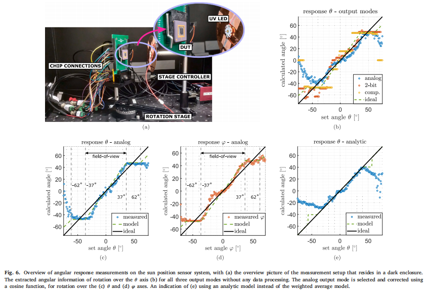
The next generation of satellites will take on the important task of addressing future challenges in communication, navigation, and observation. To achieve this goal, the number of orbital satellites is expected to continue to grow, making space exploration more cost-effective by constructing intelligent constellation systems and miniaturizing individual satellites. Ensuring that satellites possess precise autonomous navigation capabilities is crucial for these space missions. This control begins with attitude measurement using dedicated satellite sensors, typically employing sun position sensors. Current technologies face two major challenges: severe signal distortion caused by albedo reflection light from the Earth, and technical bottlenecks arising from the trend of satellite miniaturization. This study addresses these two issues by developing a silicon carbide-based micro-machined sun position sensor (utilizing wafer-level integrated optical technology). This 10mm × 10mm × 1mm system achieves an average angular accuracy of 5.7° within a ±37° field of view and integrates an on-chip temperature sensor with a K−1 type sensitivity, operating in a temperature range from 20°C to 200°C, with a magnitude of up to 3.9 mV. |
Content
Conclusion
|
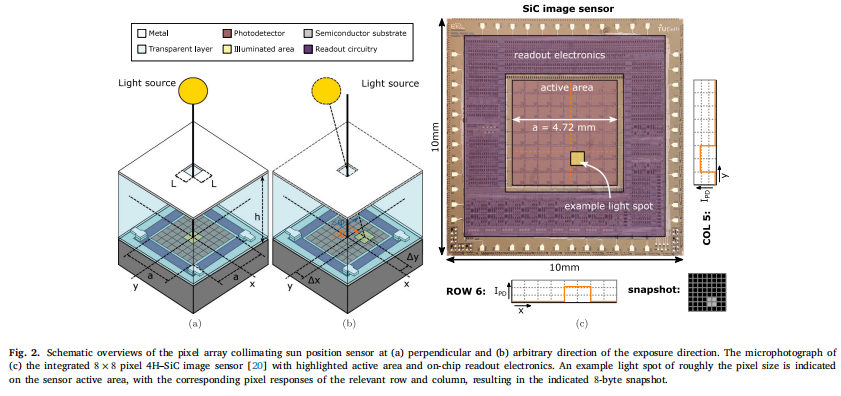
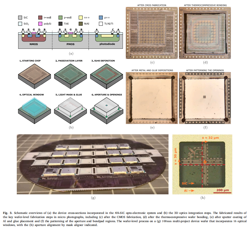
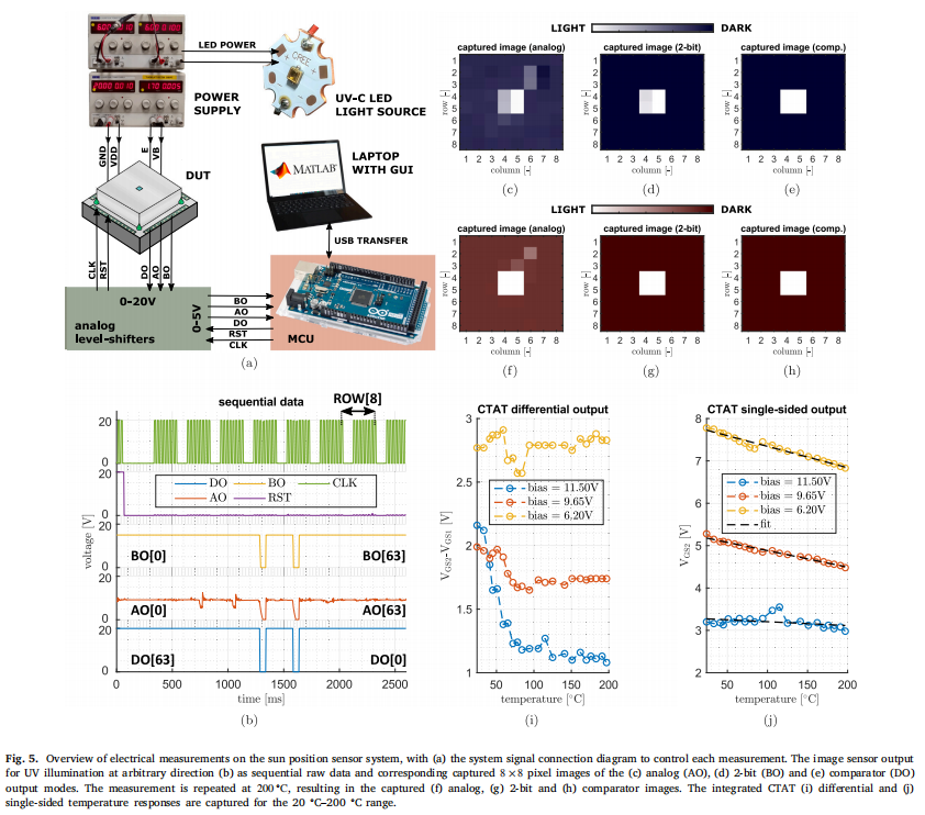
The sun position sensor system employs silicon carbide optoelectronic design, achieving a three-dimensional optical structure at the wafer level through thermocompression bonding and optical window patterning processes. Wafer-level adhesive distribution technology ensures the optical window is fixed, thereby guaranteeing high manufacturing yield. The device offers three output modes, sequentially reading and converting to an 8×8 image. The light spots captured under UV exposure extract angular information through a weighted averaging algorithm, achieving an average angular accuracy of 5.7° within a ±37° field of view. The device has been validated for normal operation at a working temperature of 200°C, with its integrated CTAT temperature sensor matching the response range. The next generation of space instruments can gain dual advantages from this: (1) the inherent UV selective response characteristics of silicon carbide photodetectors effectively suppress signal distortion caused by Earth-reflected light; (2) device miniaturization is achieved through wafer-level scalable manufacturing processes. Mass production will also reduce manufacturing costs. Future research on silicon carbide image sensor sun position sensors needs to optimize design parameters to enhance sensitivity and accuracy while ensuring broad field coverage. This can be achieved by using thicker sapphire optical windows or reducing the effective area size, thereby inherently improving sensitivity while fully utilizing the sensor’s effective area to enhance accuracy. To further improve performance, increasing the pixel count of the image sensor is necessary, which means further miniaturizing the integrated circuit module size. Finally, by considering the phenomenon of significantly reduced light power at increased incident angles (where light power is halved at a 62° angle), the field of view range is effectively enhanced. It is recommended to adopt a dynamic range scheme to adjust pixel integration time. There is also a blind spot issue in the sensor response, caused by the light spot size being smaller than the pixel size. Aligning the aperture structure with a wafer stepper can improve the sensor’s monolithic integration, although its offset has minimal impact on the current performance limits. Additionally, the wafer-level packaging process benefits from enhanced bonding strength after thermocompression bonding, thus eliminating the currently used wafer-level adhesive distribution step. |
| For submissions, please contact the editor via WeChat: 13625574907 |