1. GPIO Circuit
In the RK3588S, there are two types of GPIO that support 1.8V and configurable 1.8V/3.3V voltage levels.
2. GPIO Pin Name Description
For example, functions such as GMAC1_PPSCLK, UART7_RX_M1, SPI1_CLK_M1 are multiplexed on GPIO3_C1, and only one function can be selected during allocation.
Except for the boot-related GPIOs, the remaining IOs are reset to default input.
GPIOx_xx_u indicates that this IO reset default state is internally pulled up;
GPIOx_xx_d indicates that this IO reset default state is internally pulled down;
GPIOx_xx_z indicates that this IO reset default state is high impedance;
Each function name suffix with _M0, M1, or _M2 represents the same function multiplexed to different IOs, and only one can be selected. For example, when selecting the UART7 function, you must choose the combination of UART7_TX_M0 and UART7_RX_M0; the combination of UART7_TX_M0 and UART7_RX_M1 is not supported. This constraint applies to all functions with different IOMUX.
3. GPIO Drive Capability
In the RK3588S, GPIO provides multiple adjustable drive strength levels, ranging from most Level 0-5 and some GPIOs are Level 0-3 adjustment levels. For specifics, please refer to the RK3588S_PinOut document. Additionally, depending on the type of GPIO, the initial default drive strength may vary. Please refer to the chip TRM for configuration modifications, and also refer to the table in the RK3588S_PinOut document, specifically table 5, for “SupportDriveStrength” and “DefaultIO DriveStrength” columns.
4. GPIO Power
The power pin descriptions for the GPIO power domains are as follows:
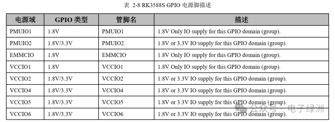
Among them, PMUIO1, EMMCIO, and VCCIO1 are fixed level power domains and cannot be configured. PMUIO2, VCCIO2, and VCCIO[4:6] power domains can automatically recognize the voltage of the hardware configuration in the RK3588S chip, and do not require software to configure based on the hardware supply voltage.
Reference Documents:
1) DTS Configuration Documentation: None available
2) Checklist: None available
Additionally, it is important to ensure that the IO levels of the power domains are consistent with the IO levels of the interfacing peripheral chips/devices;
Each power domain’s power supply pins should be placed close together with at least one 100nF decoupling capacitor; detailed design can be seen in the reference schematic, and should not be arbitrarily deleted;
If all IOs in a power domain are not used, then the power supply for that power domain can be left unpowered, and the pin can be left floating. (Except for TYPEC0)
——END——
In the jungle society, tears are never believed; no amount of complaints will help, and no one will pity you.
Recommended Reading
FA Failure Analysis Four-Step Method
Understanding Key Antenna Parameters from Scratch
SDR WDR HDR Dynamic Range
In-Depth Analysis of Rockchip RV1106B Ultra-Low Power AOV Sensor Solution
Antenna Efficiency, Antenna Gain, EIRP
Due to changes in the public account’s push rules, to prevent losing track of me, please like and star me. (Method: Go to the public account homepage, click the top right corner “…”, then click to add to stars, thank you for your support!)
Like Share AgainThank you for your “three consecutive” supportLimited time free scan to join the group, exchange more technical and industry information