Big Cat says:
Translation of Chapter 9 from the compilation “RFSoC-Book” is detailed in the first article of this series.
“An open-source masterpiece, ‘Software Defined Radio Based on Zynq UltraScale+ RFSoC'”
Mr. Big Cat, WeChat public account: Mr. Big Cat’s Little Bookshelf, an open-source masterpiece, ‘Software Defined Radio Based on Zynq UltraScale+ RFSoC’
RF ADCs on RFSoCThe advantage of RF ADCs (RF-ADCs) lies in their ability to directly digitize many modern communication signals. Additionally, the high sampling rates of RF ADCs enable applications in instrumentation, such as RF spectrum analysis of mid to low-frequency mobile/wireless spectrums, which is discussed in depth in Chapter 5. To further understand the working principles of RF ADCs, we will analyze their architecture in more detail below.1. RFSoC Chip SeriesAs described in Chapter 3, the most important feature of the RF System on Chip (RFSoC) is its integrated hard-core RF Data Converter (RFDC) module. With this module, the device can function as an RF transceiver with just additional analog circuitry and antennas. Most devices also integrate a Soft Decision Forward Error Correction (SD-FEC) module for error correction schemes. These resources, combined with programmable logic (PL) and processing systems (PS) similar to Multi-Processor System on Chip (MPSoC) devices, make RFSoC devices extremely flexible, making them ideal platforms for implementing Software Defined Radio (SDR).As of the writing of this article, three generations of RFSoC products have been released, with the first and third generations containing multiple different models. In addition to standard RFSoC devices, there is also an RFSoC DFE (Digital Front End) series optimized for 5G New Radio applications, which integrates a dedicated set of hard-core processing modules. The naming conventions for these device series are as follows:
- First Generation (Gen 1): ZU2xDR
- Second Generation (Gen 2): ZU39DR
- Third Generation (Gen 3): ZU4xDR
- RFSoC DFE: ZC6xDR
The performance of RFSoC devices can be measured by parameters such as the number of channels, resolution (the number of bits used in the quantization process), and the maximum supported sampling rate. The sampling rate determines the frequency range of the signals that can be received, while the resolution determines the background noise caused by quantization noise. Table 9.1 highlights some specifications of existing devices.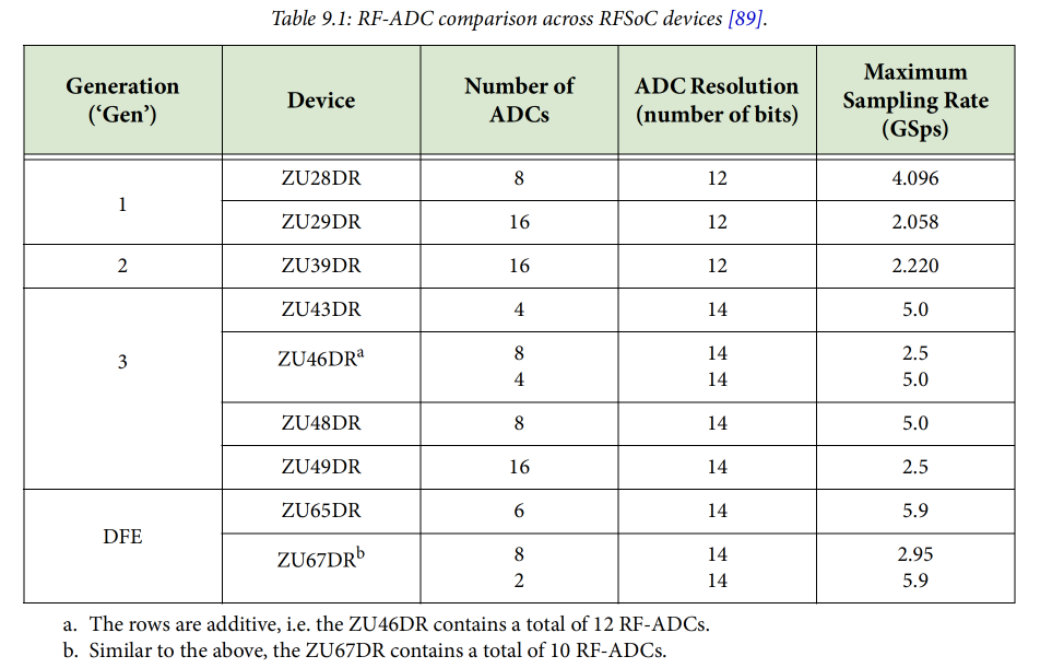 It is worth noting that the first and second generation RFSoC devices use 12-bit RF ADCs, while the third generation and DFE devices use 14-bit RF ADCs. This means that the latter has a higher resolution and therefore lower quantization noise. With each product generation, the maximum sampling rate has gradually increased. To better understand the differences within the same generation of products, we must first consider the structure of the RF Data Converter, specifically its hierarchical relationship.2. Hierarchical Structure of RF ADC TilesThe RF Data Converter (RFDC) in RFSoC devices includes RF ADCs and RF DACs, organized in a hierarchical structure of tiles and blocks. Each RF ADC and RF DAC is contained within a module, and depending on the device model, one, two, or four modules can form a tile. These tiles are correspondingly referred to as Single, Dual, and Quad tiles. Figures 9.4 and 9.5 provide high-level structural diagrams of Quad and Dual module tiles, respectively.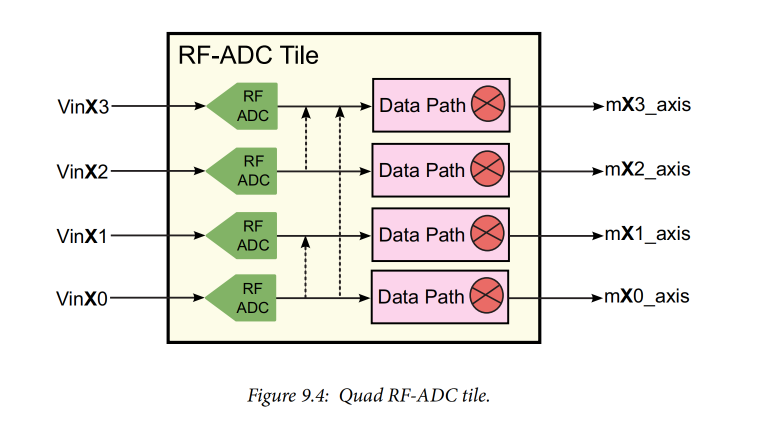
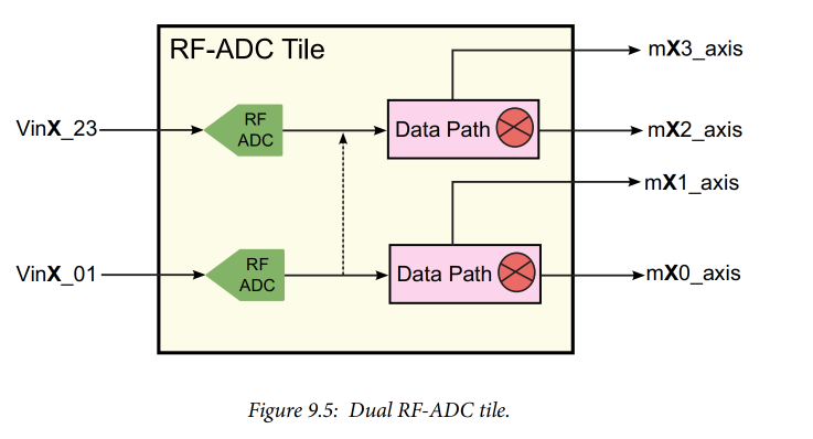 The first generation RFSoC devices may contain Dual or Quad module tiles, but each specific model only contains one type. For example, the ZU28DR device has four Dual module tiles, each containing two modules, resulting in a total of 8 RF ADCs. The second generation only includes the ZU39DR RFSoC device, which has four Quad module tiles, providing a total of 16 RF ADCs.The third generation devices may contain either Quad or Dual module tiles, or both, depending on the specific model. The ZU48DR and ZU49DR devices are similar to the previously discussed two devices, consisting of four Dual module tiles and four Quad module tiles, with a total of 8 and 16 RF ADCs, respectively. The ZU46DR device uses a mixed configuration, consisting of two Dual module tiles and two Quad module tiles, totaling 12 RF ADCs. The ZU43DR device contains four Single module tiles, each with one RF ADC, resulting in a total of 4 RF ADCs. At the time of writing this article, this is the only device using Single module tiles.The DFE devices structurally resemble the third generation devices. As of the writing of this article, there are two DFE devices on the market: ZU65DR and ZU67DR. The former contains three Dual module tiles, totaling 6 RF ADCs; the latter also contains three tiles, but consists of two Quad module tiles and one Dual module tile, resulting in a total of 10 RF ADCs.3. Interleaving FactorEach RF ADC in RFSoC devices consists of multiple sub-ADCs, and by interleaving these sub-ADCs, the maximum sampling rate can be increased. With ADC interleaving technology, multiple sub-ADCs sample the input signal simultaneously under a common clock relationship. Therefore, compared to a single ADC, interleaving m sub-ADCs can increase the effective sampling rate by m times. This multiplier m is referred to as the interleaving factor. To successfully implement interleaving, the clock phase relationship between the ADCs is crucial. This relationship can be defined as follows:
 In the equation, ϕn represents the sampling phase of the nth sub-ADC, where n=1….m.In the Dual Tile architecture, each RF-ADC consists of 8 interleaved sub-ADCs; while in the Quad Tile architecture, each RF-ADC consists of 4 sub-ADCs. Therefore, within the same generation of RFSoC, the sampling rate of Dual Tile is twice that of Quad Tile. For example, as seen in Table 9.1: the maximum sampling rate of Quad Tile in ZU46DR is 2.5 GSps; while its Dual Tile has a maximum sampling rate of 5.0 GSps. Since RFSoC offers various configuration options, designers can choose the appropriate target device based on their needs.4. Composition of RF-ADC TilesRegardless of the configuration of the tiles, each RF-ADC module contains a high-performance input buffer and a series of pipeline processing components, including: the RF-ADC itself, a Quadrature Modulation Correction (QMC) unit that can correct any imbalance in the external (analog) signal paths in the quadrature system, a complex mixer for demodulation, and a decimation filter for reducing the sampling rate. This RF-ADC processing pipeline is optimized for direct frequency conversion of RF signals.First Generation (Gen 1) TileThe structures of Quad Tile and Dual Tile are similar, with their clock circuits consisting of a Phase-Locked Loop (PLL) driven by an external reference clock. Designers can choose to enable this PLL or bypass it with an external sampling clock. All RF-ADCs within the same tile share the same clock source and infrastructure. Each RF-ADC within the tile has an associated Digital Down Converter (DDC), which includes a digital complex mixer and a programmable decimator. This decimator contains a series of half-band filters that can be programmed to achieve overall decimation factors of 1, 2, 4, or 8. Each RF-ADC within the tile has its dedicated mixer and decimator.
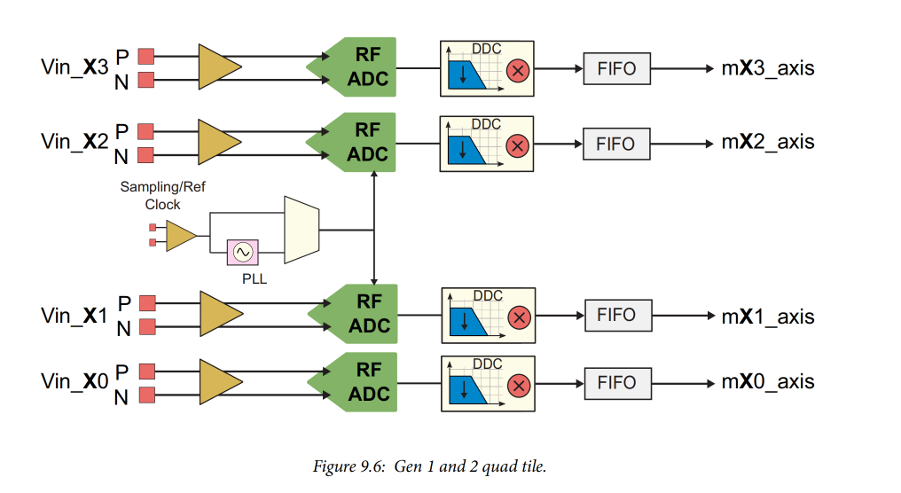 As shown in Figure 9.6, the Gen 1 Quad Tile contains four RF-ADCs arranged in pairs. Each RF-ADC can be configured to operate independently (for processing real signals) or in pairs (for processing complex signals).
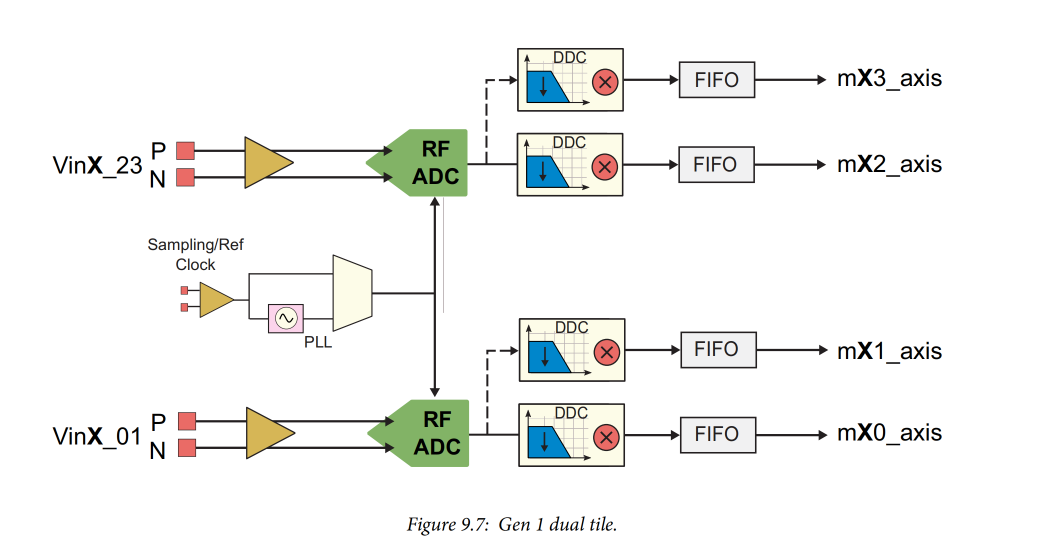 Figure 9.7 shows the configurations of Gen 1 and Gen 2 Dual Tiles. It is very similar to Quad Tile, but contains only two RF-ADCs. These two RF-ADCs can operate independently or in pairs to receive complex signals. Complex signal reception can only be achieved when the RF-ADCs within the tile operate in pairs. In this mode, the even-numbered RF-ADCs process I-channel data, while the odd-numbered RF-ADCs process Q-channel data.Now, we can simplify the operation of each RF-ADC module within the tile and its associated DDC into a single linear pipeline, as shown in Figure 9.8.
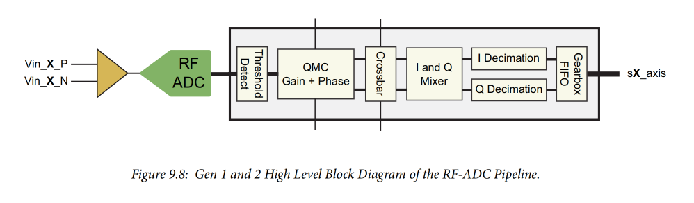 The steps of this processing pipeline are as follows. The RF-ADC can be highly controlled through the RFDC interface, providing designers with significant operational flexibility at each stage.
- After entering the buffer, the analog signal is sampled and converted into a digital signal by the RF-ADC at a specific acquisition rate.
- Subsequently, a threshold detector can be used to detect and record the amplitude level of the input signal.
- If the received signal is in complex form, the QMC module can compensate for any imbalance between the I and Q signal paths.
- Next, the complex mixer down-converts the input signal to baseband for further processing.
- Finally, the decimators for the I and Q channels can decimate the signal and then connect to the PL (Programmable Logic) via the Gearbox FIFO interface.
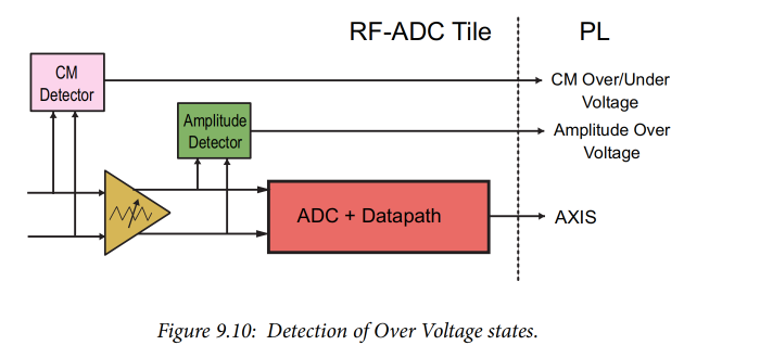
Third Generation (Gen 3) TileThe operation of the Gen 3 Tile is similar to that of the Gen 1 and Gen 2 Tiles, with high-level functions resembling those in Figure 9.8. The Gen 3 Tile adds a digital step attenuator (DSA) at the RF-ADC front end. Additionally, the Gen 3 Tile provides a more advanced decimation filter chain, supporting decimation factors of 1x, 2x, 4x, 6x, 8x, 10x, 12x, 20x, 24x, and 40x.When the amplitude or power of the analog signal varies over time, the DSA can adjust it to the optimal input range of the RF-ADC. For example, such power variations may be caused by fluctuations in received signal strength or interference signals. Traditionally, the DSA is usually an external component (such as a variable gain amplifier), but in the third generation devices, this function is integrated with the internal input buffer, as shown in Figure 9.9.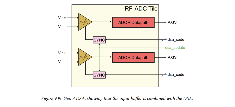 The DSA is also used to automatically prevent over-voltage conditions (input signals that are too large, exceeding the RF-ADC processing range). This situation can occur in two forms: “Over Amplitude” and “Outside Common-Mode Range.” For the “Over Amplitude” case, when the signal amplitude in the input buffer is too large for the RF-ADC, a flag in the buffer will trigger the DSA and automatically set it. “Outside Common-Mode Range” is triggered when the input value is above or below a reliable common-mode range. In this case, the input buffer can be disabled for self-protection. These over-voltage protection functions and the relative position of the DSA are shown in Figure 9.10.
 The third generation RF-ADC also supports clock distribution between the RF-ADC and RF-DAC, as shown in Figure 9.11. In normal operating mode, each tile runs using its independent tile clock. As previously mentioned for the first generation, this clock can be sourced externally or generated by an on-chip PLL. The “clock distribution” feature allows one tile to distribute its clock in a chain structure to other adjacent tiles. However, note that only RF-ADC 1 and RF-ADC 2 can serve as sources for high-frequency clock distribution (RF-ADC 1 is recommended).
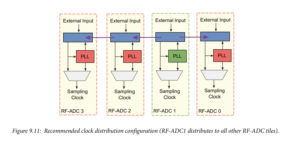 As long as the link is not interrupted by other clocks, this clock can be forwarded to any number of adjacent tiles. In the example shown in Figure 9.11, RF-ADC1 can distribute its clock to RF-ADC0, and it can also distribute to RF-ADC2, which can then distribute to RF-ADC3. The clock must first be distributed to RF-ADC2 before it can be distributed to RF-ADC3.