In modern electronic systems, the design of Radio Frequency (RF) circuit boards has become increasingly complex and critical. With the rapid development of communication technologies, from 5G mobile communications to satellite communications and radar systems, the performance of RF circuits directly affects the quality and reliability of the entire system.
The design of RF circuit boards is a meticulous and complex task that requires consideration of many special factors.
During the design process, impedance matching is the most fundamental requirement. The RF signal path must maintain a consistent characteristic impedance, typically 50Ω. Any point of impedance discontinuity will lead to signal reflection, thereby reducing system performance. For microstrip lines or strip lines, impedance can be controlled by adjusting the line width and dielectric thickness; for differential lines, the spacing between the lines must also be considered. In practical applications, using impedance calculators or electromagnetic simulation software to accurately calculate impedance is an essential step.
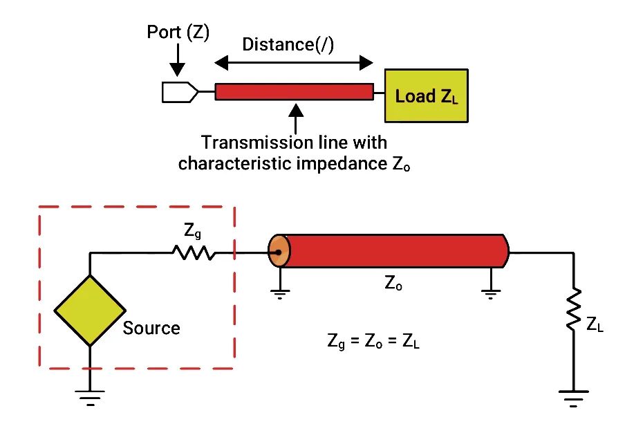
The characteristic impedance of the transmission line must match the load to achieve maximum power transfer.
Good grounding design is crucial in RF circuits. A large area, low-impedance ground plane should be used, avoiding slots and cuts in the ground plane. For high-frequency sections, it is recommended to use dense vias to “stitch” multiple layers of ground planes together and place ground vias on both sides of the signal lines, especially in circuits with frequencies exceeding 1GHz. This design can effectively reduce ground impedance and minimize electromagnetic interference.
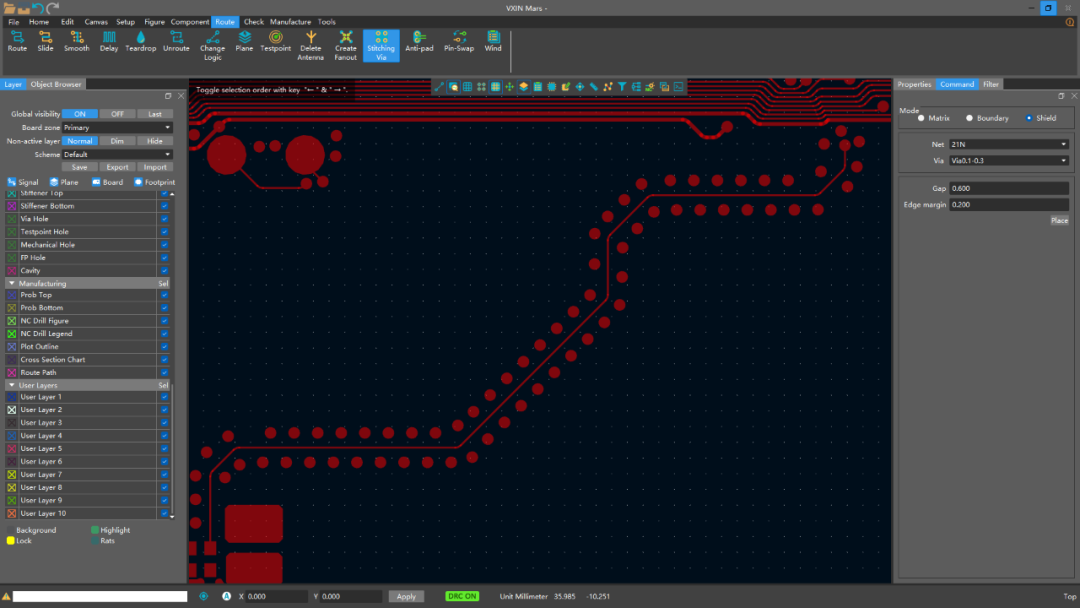 For Vxin Mars PCB software – via stitching
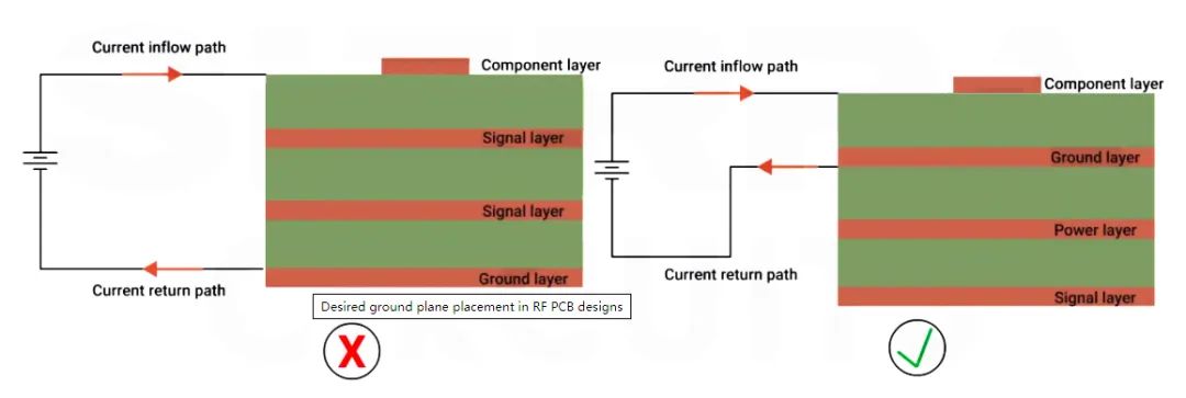
The required ground layout in RF PCB design
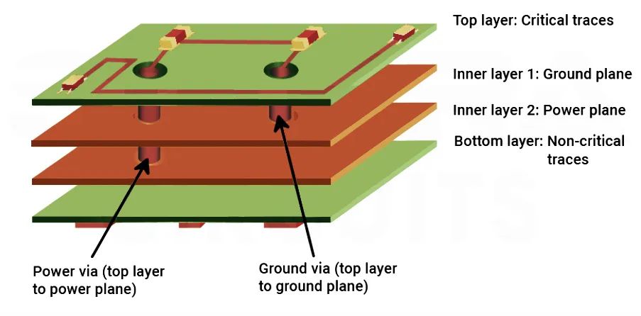
RF PCB stack layout
The layout of components and routing has a direct impact on RF performance. Designers should minimize the length of critical signal paths and maintain the natural flow of signals. In routing design, sharp angle bends should be avoided, and 45° angles or curved traces are recommended to reduce reflections and radiation. Sensitive circuits such as Voltage Controlled Oscillators (VCO) and Low Noise Amplifiers (LNA) should have dedicated shielding areas, while high-frequency components should be placed as close as possible to their associated decoupling capacitors to minimize parasitic effects.
To avoid interference between circuits, isolation and shielding techniques are essential. Digital and analog/RF sections should be separated, using ground via walls to isolate different circuit areas. For particularly sensitive circuits, consideration should be given to using metal shielding enclosures for additional protection. There should be sufficient isolation between high-power RF areas and low-noise circuits to prevent unnecessary cross-interference.
Transmission line design needs to select the appropriate type based on frequency and layer structure. Microstrip lines are simple and practical but have higher radiation losses; strip lines have better shielding performance but are relatively complex to manufacture; while coplanar waveguides can provide better performance and flexibility in certain applications. Designers need to weigh these factors based on specific application scenarios.
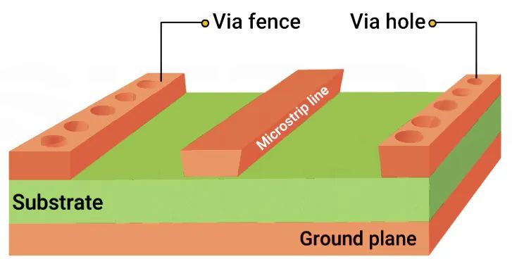
Through the fence in microstrip lines
RF circuits are particularly sensitive to power quality, and good power integrity design cannot be overlooked. Layered power planes should be used, and multiple decoupling capacitors of different values should be placed near each power pin. For critical RF components, dedicated low-noise regulators may need to be considered, while power filtering and isolation networks are also important means to ensure clean power.
Thermal management is another key factor in RF circuit board design. RF power devices generate a lot of heat, and copper-clad areas can be used to provide heat dissipation paths, while heat via arrays should be considered for high-power devices. During the design process, the thermal expansion and mechanical stability of components must also be considered to ensure reliable operation of the circuit under various environmental conditions.
Finally, RF circuits are very sensitive to manufacturing tolerances, so special attention must be paid to material selection and manufacturing specifications. Materials suitable for RF applications, such as Rogers or Taconic specialized RF materials, should be chosen, and the dielectric constant and loss tangent tolerance requirements should be clearly specified. At the same time, the consistency of copper thickness will also affect impedance control, and controlled impedance testing may be considered for critical traces to verify the design.
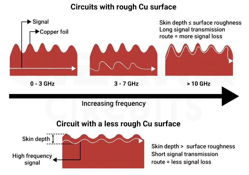
The impact of copper foil surface roughness on high-frequency signals
In the actual design process of RF circuit boards, engineers need to comprehensively consider the above factors based on specific frequency ranges, power levels, and application requirements to design RF circuit boards that are high-performing and reliably stable.
Selected by Vxin
2025

▲ Current applications of AI in the EDA industry

▲ The impact of PCB chamfering on signal quality
Vxin Technology Co., Ltd.
Domestic EDA solutions for electronic product R&D
www.vxintech.com
400-009-0858
18939865283
Follow Vxin