


Click the blue text above to follow us


1. What is I2C?
I2C, short for Inter Integrated Circuit, is a two-wire serial bus developed by Philips for communication between SOCs and peripherals. It requires only two wires for communication, operating in a master-slave mode where the master can read and write data, while the slave can only wait to be read or written to. The slave has no autonomy.
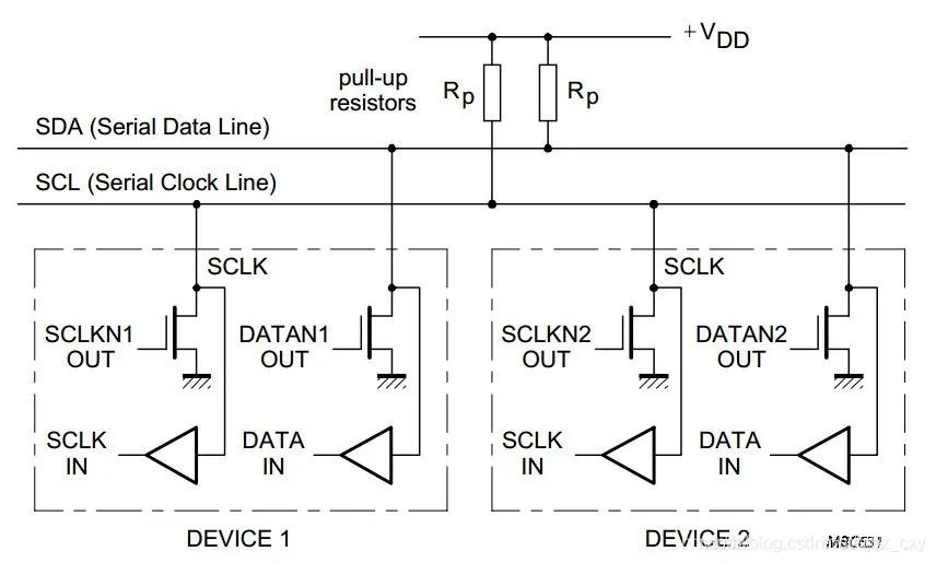
I2C allows for bidirectional communication through two lines: SDA (Serial Data Line) and SCL (Serial Clock Line). The interface outputs are open-drain, and the bus interface is integrated within the SOC. We just need to find its interface on the schematic and connect it to the peripherals using Dupont wires or other methods to achieve I2C communication.
Both SDA and SCL are externally connected to pull-up resistors, so when SDA is idle, it always outputs a high level. It also imposes certain requirements on peripherals, which must also have an open-drain output mode, as this relates to the circuit implementation. If the two circuit interface modes differ, normal communication will not be possible.
The pull-up resistors in I2C are not arbitrary; the higher the resistance value, the longer the signal pull-up period, which increases the communication cycle time and decreases the speed.
I2C provides each device with an address, which can be used to identify different devices. Only when a slave device receives its own address does it respond.
Since many devices can be connected to I2C, each slave must set its own address, while the master does not need to, as it is not read or written by slave devices; the master is responsible for reading and writing to other devices.
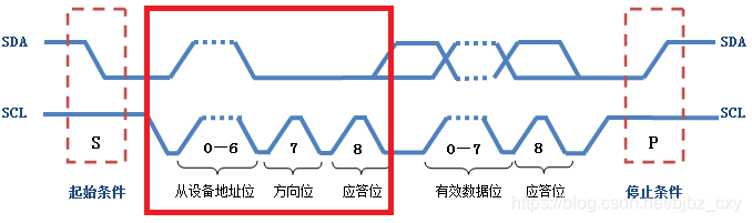
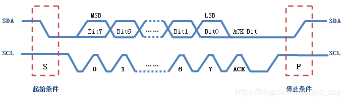
Communication begins with a start signal, which consists of 9 bits: the first 7 bits are the slave device address, and the last bit indicates the direction (0/1 for read/write).
This indicates that the address of a slave device cannot exceed 7 bits.
2. I2C Composition Principles
Architecture diagram:
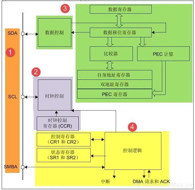
The SMBA line is used for SMBUS warning signals, which are not utilized in I2C communication and can be ignored.
I2C has its own control unit for handling communications, which can be considered a small chip that is integrated into the SOC (some architectures may not include it).
3. I2C Characteristics
-
Requires only two wires
-
Interface integrated within the PCB
-
Due to open-drain output, power consumption is low (high current is handled by pull-up resistors; generally, devices do not need to output high levels, so this part has low power consumption)
-
World-class standard, most development boards support it
-
One-to-many: one line connects multiple peripherals, distinguished by addresses, saving layout space
4. I2C Communication Modes
Bidirectional transmission bus:
|
Mode |
Speed (kbit/s) |
|---|---|
| Standard-mode | 100 |
| Fast-mode | 400 |
| Fast-mode Plus | 1M |
| High-speed mode | 3.4M |
Unidirectional transmission bus:
|
Mode |
Speed (kbit/s) |
|---|---|
| Ultra Fast-mode | 5M |
These modes are determined by the speed. Setting the I2C communication speed to match the corresponding rate means it operates in that mode. However, there is a delay because the signals pass through pull-up resistors, which depend on the resistor values; the signal experiences a periodic change when passing through the pull-up resistors.
Setting method: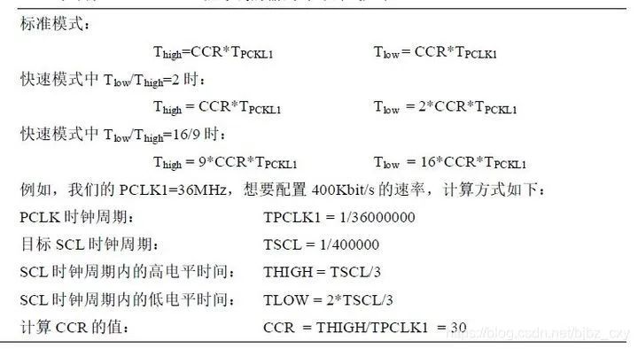
We need to calculate based on the current PCLK clock frequency, similar to setting the PWM duty cycle, requiring calculations to set the value of the I2C CCR clock control register. If the frequencies differ, normal operation cannot occur.
For example: if the clock frequency is 66MHZ, the prescaler value is 65MHZ, and the coefficient is 1/2, the calculation formula is as follows:
Clock frequency = PCLK / ((prescaler value + 1)) / division coefficient
We know PCLK is 66, the prescaler value is set to 65, and the division coefficient is 1/2, meaning we divide by 2.
So the formula becomes: 66 / (65 + 1) / 2 = 0.5
Converting 0.5 to Hz: 0.5 * 1000 = 500KHZ. There is also a formula for converting Hz to seconds; the reciprocal of Hertz gives its seconds, expressed as: (1/500) = 0.002ms, 1 millisecond = 1000 microseconds, 0.002 milliseconds equals 2 microseconds. Using this formula, we can determine that our current frequency is working once every 2 microseconds.
If we want it to work every 0.5 milliseconds, then TCNTB’s value = 500 milliseconds / current microsecond frequency 2.
500 / 2 = 250, so TCNTB’s value should be 250. Alternatively, this can also be calculated as: 2 microseconds once, 1 millisecond = 1000 microseconds, 0.5 milliseconds equals 500 microseconds, 500 microseconds / 2 microseconds = 250. After 250 cycles of 2 microseconds, we reach 500 microseconds, which equals 0.5 milliseconds.
5. I2C Communication Process
Communication steps:
-
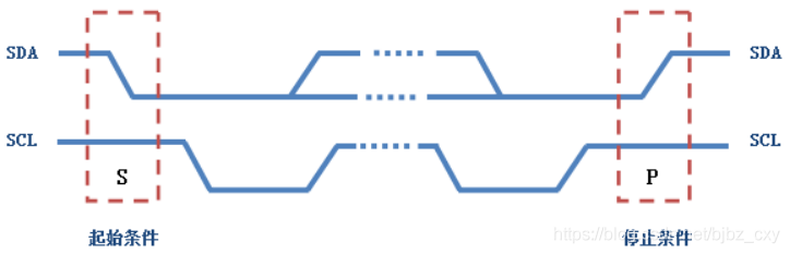
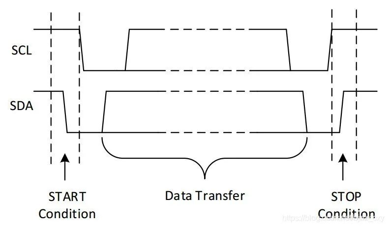
Start signal: SCL is high while SDA transitions from high to low, indicating a start condition
-
Stop signal: SCL is high while SDA transitions from low to high, indicating a stop condition
-
Acknowledge signal: After sending a signal, it is pulled low
In the idle state, SCL and SDA both maintain high levels.
Among these three signals, the start signal is mandatory, while the stop and acknowledge signals can be omitted based on the situation.
After the start condition is generated, the bus is busy, exclusively occupied by the master and slave devices for this data transmission, preventing other I2C devices from accessing the bus. After the stop condition is generated, the master and slave devices release the bus, returning it to an idle state.
Transmission process:
-
Each time data/address is transmitted in 9 bits, with the first 8 bits being data and the last bit being the acknowledge bit
-
Transmission is high-first, low-later
-
The master pulls SDA low while SCL and SDA are both high, creating a falling edge signal on SDA. The slave detects this and knows the master has sent a start signal, prompting the slave to pull the SDA line high to signal readiness
-
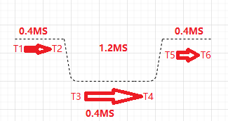
This level change does not refer to a change at a single point in time; for example, if the previous second was high and the next second is low, this does not count as a change. A change at a time point requires that during one cycle, a certain period is high, and another period is low. Completing such an action during the entire cycle constitutes a rising or falling edge change, which depends on the I2C clock frequency.
-
As illustrated, if one cycle is 1.2 milliseconds, the periodic changes within that millisecond are as follows:
-
Between T1 and T2, the signal is high, and between T3 and T4, it is low. The entire cycle then becomes a falling edge signal.
-
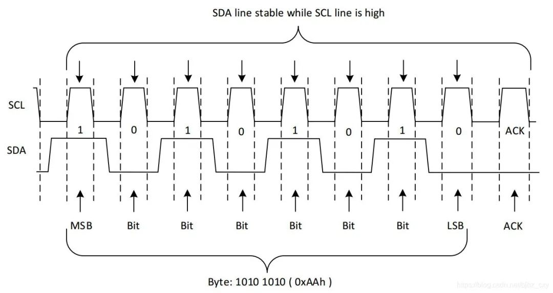
The master generates clock pulse signals on the SCL line, sending out a data bit on the SDA line with each pulse. The slave detects the pulse signal and reads a BIT from the SDA line. After generating the pulse signal, SCL is low, allowing the SDA level to change according to the transmitted digital signal (to prevent data instability, the SDA is only allowed to change level when SCL is low; after sending a pulse signal, SCL requires pulling low).
Initially, the address information is sent, with each valid bit being 8 bits. After the master sends 8 bits, it will not send more, and after sending the eight bits, it will keep the SDA line high (since the BIT being sent may be high or low, and the 8th bit could be low, it must be pulled high again). Then it waits for the slave to pull low; upon detecting this, the master considers the communication successful.
-
Next, data bits can be sent similarly to address information, where SCL generates pulses and SDA flips. After sending is complete, a stop bit is generated by the master, which pulls SCL high to keep it high, then changes SDA periodically: rising edge, meaning it pulls low for a certain period and then pulls high. At this point, both SCL and SDA are in high-level mode, indicating the bus is idle and can be occupied by other devices.
The slave device must continuously monitor the SCL level changes to complete corresponding actions.
Below is the transmission timing for sending 170 (hex: 0xAA; binary: 1010 1010) to the slave device:
To summarize the understanding of start and stop signals:
-
Start condition: When SCL is high, SDA transitions from high to low.
-
Stop condition: When SCL is high, SDA transitions from low to high.
There is also a repeated start condition, which does not require a stop symbol; simply sending a repeated start condition allows any byte of data to be sent afterwards. When all data has been sent, a stop condition is sent.
-
This means sending a Sr signal to the slave without releasing the bus, followed by repeating the last transmission. The advantage of this is to prevent other devices from seizing the bus during transmission, as there is a certain idle time after each transmission. If this idle time is occupied by another device, it can result in incomplete data transmission, since each transmission only sends one byte of valid data, and each communication must generate start and stop signals, leading to some idle time.
For specific communication steps, refer to the official I2C documentation.
6. I2C Interface Working Modes
There are four working modes for the I2C interface
|
Working Mode |
Description |
|---|---|
| Slave Transmitter Mode | When the slave device receives the ADDR address from the master, it sends the value from its internal data register to the SDA bus via the data control module. This mode is generally used when the master reads data from the slave. |
| Slave Receiver Mode | When the slave device receives the ADDR address from the master, it stores the data from the SDA bus into its data register via the data control module. |
| Master Transmitter Mode | After sending the ADDR address and receiving a response from the slave, it sends the value from its data register to the SDA bus. |
| Master Receiver Mode | After sending the ADDR address and receiving a response from the slave, it writes the data from the SDA bus into its data register. |
The data register is typically the DR register (Data Register), which is waiting for the internal program to read from it.
Since data is sent from high to low, there is an internal shift register process to write into the DR register.
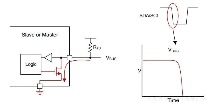
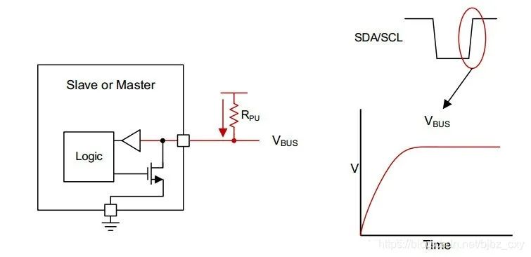
7. Hardware Pull-Up and Pull-Down Process
Both SDA and SCL of I2C are externally connected to pull-up resistors. If they remain in a pulled-up state, they can only output a high level and cannot output a low level, leading to incorrect logic signal clock levels. Therefore, a pull-down process is necessary to ensure the transmitted bit is valid and correct.
Internally, I2C has a logic controller responsible for this control. When a pull-up is needed, it controls the FET (Field Effect Transistor, primarily used to control semiconductor devices and resistance values) to lower the pull-up resistance value, ensuring the current remains in a low level range, generating a low level signal.
Pulling Down:
Pulling Up:
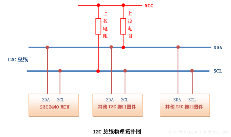
The physical layer topology of S3C2400 (for reference only):
8. One-to-Many
I2C assigns an address to each slave device, allowing the master to select which slave to control by sending the address bits.
Each slave connected must set its own address for the I2C master to find it.
Each device connects to the SDA and SCL of I2C, and the I2C master sends addresses over these lines. When a slave receives an address, it determines whether it is the one being sought.
The connection diagram below shows all devices connected to the I2C master device, meaning the SDA and SCL of the I2C master are brought out, and the slave devices are connected to these lines. When data is sent, all devices on this line can monitor the level changes, similar to socket broadcasting.
The master device does not need to set its own address, as it will not be sought by others. However, if it needs to cooperate with other peripherals, it can set its own address and write listening code to act as master or slave.
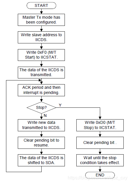
9. Development Process
Host Receive Mode:

Host Send Mode:
Click to view, you look the best