MIPI (Mobile Industry Processor Interface) is the abbreviation for Mobile Industry Processor Interface, an open standard initiated by the MIPI Alliance for mobile application processors.MIPI uses a high-speed serial interface to transmit data, meeting the transmission requirements of high-resolution cameras. The use of a serial interface facilitates PCB layout and wiring, improves signal integrity, and helps reduce PCB area.The MIPI interface cameras are generally small in size, suitable for compact embedded devices such as smartphones and dash cameras, and are also widely used in AI inference devices.This article introduces the development of MIPI-related technologies using Baidu’s EdgeBoard as a prototype for on-device inference equipment.If users purchase the EdgeBoard, the factory image includes MIPI functionality, and they only need to buy the recommended MIPI camera for plug-and-play operation.MIPI IntroductionThe MIPI interface is divided into two categories: DSI (Display Serial Interface), which provides a high-speed serial interface between the processor and the display module; and CSI (Camera Serial Interface), which provides a high-speed serial interface between the processor and the camera module. This article will introduce CSI-2.MIPI signals use low-voltage differential signaling for transmission, characterized by fast transmission rates and strong anti-interference capabilities. MIPI’s transmission modes are divided into low-speed signal mode and high-speed signal mode, with low-speed signals used for control commands (10 MHz) and high-speed signals for data transmission (80 Mbps – 1 Gbps/lane). The clock operates in a non-continuous state, switching according to the transmission state, which can greatly reduce power consumption. For more information on D-PHY, refer to the MIPI® Alliance Specification for D-PHY.MIPI can support up to 4-channel data, with an IIC bus for configuration. The transceiver interface is shown in the figure below: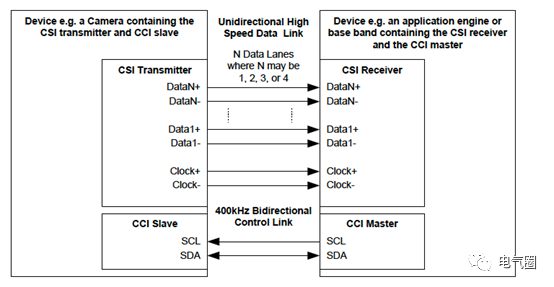 The MIPI protocol also adopts a structure similar to Ethernet protocols, using a layered design concept, divided into PHY Layer, Protocol Layer, and Application Layer.
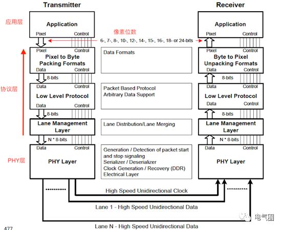 The messages transmitted via MIPI define the type/format of image data (Data type), which helps determine whether the link is functioning correctly during debugging. Common Data Types are shown in the figure below; for example, the identifier for YUV data format ranges from 0x18 to 0x1F, with the values in between defining specific formats such as YUV422, YUV444, etc. For more details, refer to the MIPI Alliance Specification for Camera Serial Interface 2.
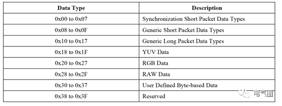 Hardware RelatedMIPI LevelsThe MIPI level standards are divided into LP (Low Power) mode and HP (High Power) mode. In LP mode, the maximum high level is 1.3V, the minimum is 1.1V, and the typical value is 1.2V. In HP mode, the common mode level is 200mV, with a swing of 200mV.
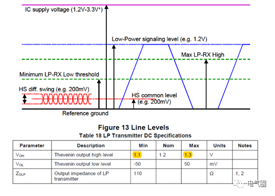 D-PHY1. The Ultrascale series FPGAs use MIPI_PHY_DCI levels, with digital control impedance. If the MIPI data rate is very high, for example, if the lane rate exceeds 1000 Mbps, a 100R termination must be enabled.2. If using K7 series chips, since they do not support MIPI_PHY_DCI levels, they can be converted from LVDS levels. Refer to Xilinx’s official document D-PHY solutions XAPP894 for a complete D-PHY layer solution.
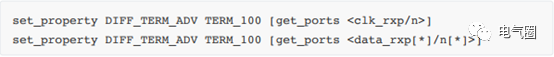
Note 1: For versions of Vivado below 2018.2, if the MIPI line rate is very high, such as 1500 Mbps, termination constraints need to be added in the xdc constraint file for Ultrascale chips. Perform the following operations:
 MIPI Pin Assignment and BANK Voltage1. The EdgeBoard uses Xilinx Ultrascale+ series MPSoC, and the MIPI IO must be placed in the HP Bank.
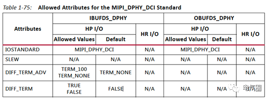 2. The MIPI_PHY_DCI level has strict requirements for the Bank; the VCCO of the Bank must be set to 1.2V, and the BANK’s VREF is recommended to be connected to 240R. If there are other level standards in the Bank, such as 1.8V levels, errors will occur during implementation.
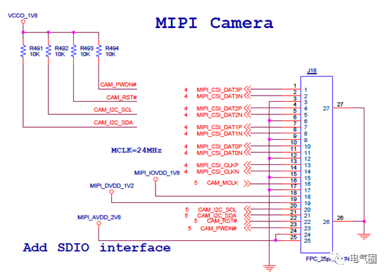
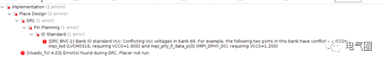 3. The MIPI-CSI-RX IP has a Pin assignment function that can verify pin assignments, refer to the MIPI IP configuration below.LayoutThe D-PHY standard specifies that the total transmission delay must not exceed 2 ns, corresponding to a maximum trace length of 25cm to 30cm for FR4 material PCBs, including from the transmitter to the receiver. This determines that the transmission distance supported by MIPI is around 30cm, refer to AN-1337D-PHY. Meanwhile, PCB traces must match a 100-ohm termination.EdgeBoard‘sMIPI The MIPI of EdgeBoard supports up to 4 channels, which can be selectively used as needed. Users can connect via ribbon cables to the EdgeBoard, noting that the ribbon cable should not be too long, preferably less than 10cm.
 DevelopmentVivado The video IP in the Vivado tool is also gradually being developed and improved, and various unexpected bugs are inevitable. Fortunately, Xilinx’s official forum is well maintained; as long as you post a question, you will receive a response from dedicated technical personnel in a short time. Additionally, Xilinx regularly releases corresponding patches for the bugs that arise, and various posts accumulated in the Video forum provide solutions for subsequent developers.1. If using Vivado version 2017, the MIPI CSI RX IP cannot handle the issue of missing MIPI camera clock. Refer to AR70581. To resolve this issue, refer to AR70530 for the patch. After successfully applying the patch, the Vivado software interface will prompt AR70530. If using versions after 2018, this issue does not exist, and no patch is needed.
 2. The MIPI-CSI-RX license needs to be purchased for use. During the verification phase, an Evaluation license can be applied for on the Xilinx official website, but the bit file generated with the evaluation license will intermittently stop working and cannot be used in actual products.License application reference is provided in the following section for applying for the Xilinx Evaluation License3. There is also open-source MIPI CSI2 IP available on GitHub, which targets Xilinx 7 Series FPGAs and can support up to 4K resolution, developed in VHDL, but only supports 4-channel MIPI cameras.4. It is recommended to use version 2018.3 and above for MIPI development.MIPI IP Configuration1. Basic settings should be made according to the parameters of the MIPI camera, mainly including color format, number of channels, line rate, etc. The line rate should preferably be higher than the rate of the MIPI camera. The MIPI IP has an internal FIFO buffer for data, ensuring that the read rate of the MIPI IP is higher than the write speed of the MIPI camera to prevent frame loss.
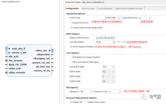 2. Pin verification must be conducted before hardware design, as MIPI has relatively strict requirements for pins, so caution is advised.
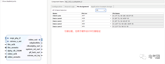 MIPI Post-Processing IP The previous MIPI IP is only responsible for obtaining data from the front-end camera; other IPs are needed for subsequent processing to obtain complete video.Demosaic also known as interpolation, constructs a standard color image through interpolation algorithms using the colors of adjacent pixels, achieving conversion from Bayer to RGB.The output of each pixel from the camera’s photosensitive sensor is not standard RGB; each pixel is only one of the three primary colors, and the standard RGB is restored through interpolation algorithms in the backend ISP. This method was proposed by Kodak scientist Dr. Bayer and is known as the Bayer filter.The photosensitive sensor contains a color filter array (CFA), which filters out the color of a single pixel by placing different primary color filters. Each pixel is a single color (one of RGB), also known as RAW data, which is restored to standard RGB through interpolation algorithms in the backend ISP. The following figure shows two filtering methods, one is RGB, and the other is CMY (printing four-color color mode).
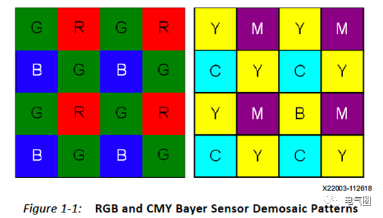 NOTE: When using the Demosaic IP, it is necessary to specify the color of the first pixel in the upper left corner of the sensor, as different sensors have different starting pixel colors. This is set in the Demosaic’s BAYER_PHASE (0x0028) Register, refer to the document SensorDemosaic.IP configuration is as follows: set the number of pixels per clock, pixel data width, and resolution.
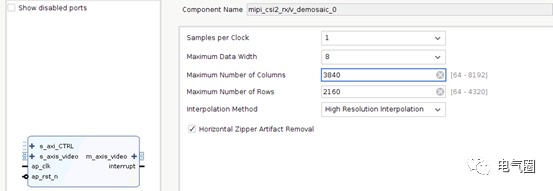 Gamma Correction The purpose of gamma correction is to adjust linear brightness signals or RGB encoding into non-linear data suitable for display. The IP uses a Gamma LUT, which is free, and specific configurations are shown in the figure below.
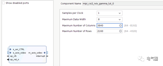 Video Process Subsystem The Video process subsystem IP has various video processing functions, and for MIPI, color space conversion can be used to achieve YUV444 or RGB color correction, enhancing visual effects.
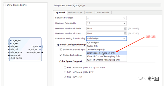 Note: The above IP settings are based on Vivado version 2017.4, and versions 2018 and above may differ slightly. Based on our development experience, we recommend using version 2018.3.EdgeBoard MIPI Camera Data Stream The MIPI camera data stream in EdgeBoard is shown in the figure below. When users purchase the EdgeBoard and pair it with our recommended MIPI camera, it can achieve plug-and-play functionality.
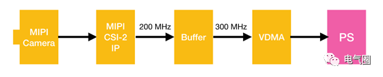 Key Registers The Xilinx MIPI IP and D-PHY are black boxes for developers. If issues arise during development, they can only be tracked through registers. Here are some key registers. By tracking the status of these registers, problems can be located and diagnosed.D-PHY Key RegistersFirst, check the working status of D-PHY. In the MIPI IP settings, the Enable D-PHY Register Interface must be enabled.1. Control Register1. Check if D-PHY is enabled2. CL_STATUS Register (CL -> Clock Lane)1. Check if the clock lane is in stop state2. Check if the channel has completed initialization3. Check the working mode3. DL_STATUS Register (DL -> Data Lane)1. Check if the data lane is in stop state2. Check if the channel has completed initialization3. Check the working modeCSI2-RX Key Registers1. Core Configuration Register1. Enable core2. Protocol Configuration Register1. Lane number: If there are no hardware issues, the number of channels used by the MIPI camera can be seen3. Core Status Register1. Count the received packets4. Check if the FIFO is full; if data is read out in time, it will not be full5. Interrupt Status Register1. This is an important register for troubleshooting; various issues that cause interrupts will be written to this register6. If ECC errors occur, it is likely a hardware signal integrity issue7. Generic short Packet Register1. Check the image format; the correct Data Type can be seen in this register, indicating that the hardware design is likely fine8. Clock Lane Information Register1. Check the working status of the clock9. Lane Information Register1. Check the working status of each lane; each lane is not always in working status and may also be in inactive stateAppendix: Application for Xilinx Evaluation License1. First, you need to have an official Xilinx account, then go to the Evaluation License website to apply. The application interface is as follows:
 2. Click search now, enter the keyword mipi, and check MIPI RX
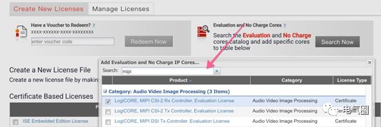 3. The Evaluation License needs to be bound to the MAC address of the host. Click Generate Node-Locked License, then set the MAC address to be bound.
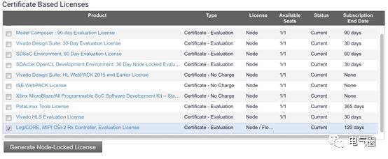
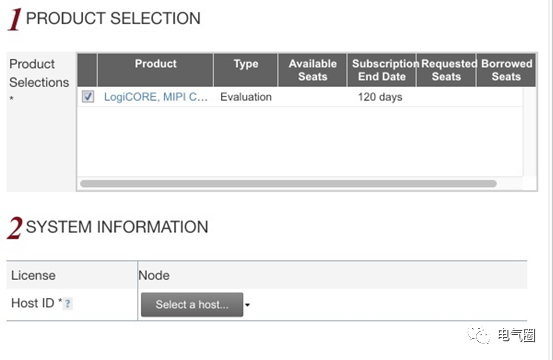 4. You will soon receive a lic file released by Xilinx in your registered email, which can be imported into the Vivado tool.NOTE: The Evaluation License is limited to testing the MIPI IP and MIPI camera’s working status and cannot be used for product release, as it contains a counter that will stop working after continuous use for several hours.