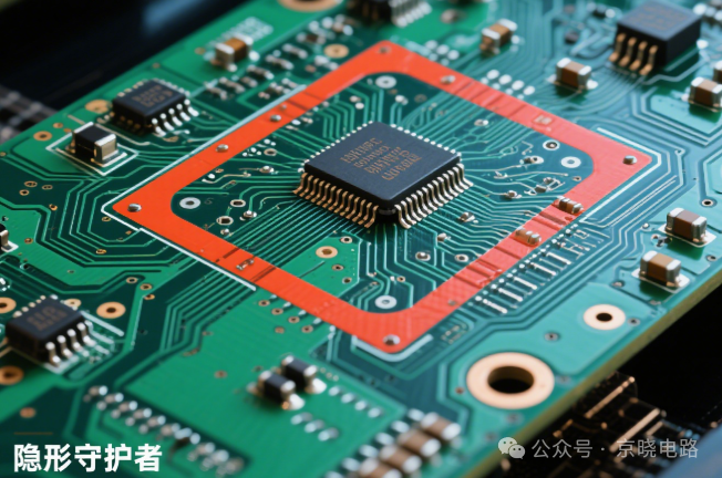
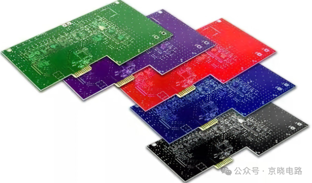
In the wave of precision and miniaturization of modern electronic devices, printed circuit boards (PCBs) serve as the core carriers of electronic systems, and their performance directly affects the success or failure of products. Solder mask design, as a key part of PCB design and manufacturing, acts like an “invisible guardian” hidden beneath the circuits. It not only isolates external corrosion through an insulating protective layer, ensuring stable electrical performance of the circuits, but also enhances production yield by precisely controlling the soldering areas. Moreover, with a variety of color options, it gives circuit boards a unique appearance. From consumer-grade smart terminals to aerospace-grade precision instruments, solder mask design is reshaping the reliability and functionality of every circuit board with its unseen power. Below, we will delve into the purposes, design points, manufacturing processes, and the creation of solder mask bridges to analyze what solder mask design is.
 Purposes of Solder Mask
(1) Protecting Circuits and Enhancing Electrical Performance: In complex usage environments, PCBs are susceptible to corrosion from moisture and various chemical electrolytes. The solder mask layer acts like a “protective suit” for the circuits, effectively preventing oxidation and corrosion, avoiding electrical performance degradation due to corrosion, and ensuring stable operation of the circuits. In humid industrial environments or electronic devices near the sea, the solder mask layer can significantly extend the lifespan of the PCB.
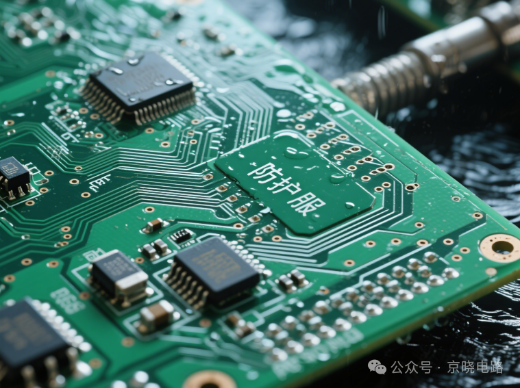
(2) Preventing Mechanical Damage and Ensuring Insulation Performance: During the production, installation, and use of PCBs, they inevitably suffer from mechanical scratches. The solder mask layer can prevent external mechanical scratches, avoiding short circuits caused by scratches between circuits, maintaining good insulation performance on the board, and ensuring the safety and reliability of electronic devices.
(3) Precise Control of Soldering Areas to Avoid Short Circuits: When soldering components on circuit boards, precise control of the soldering areas is crucial. The solder mask layer can prevent unintended areas from being connected by solder, effectively avoiding short circuits and ensuring that each solder point is accurate, thereby improving soldering quality and production efficiency.
(4) Reducing Costs and Saving Resources: The solder mask layer can reduce the loss of tin spraying or gold plating in non-soldering areas. By precisely covering areas that do not require surface treatment, unnecessary material waste is avoided, lowering production costs and improving resource utilization.
(5) Beautifying Appearance and Enhancing Product Image: The solder mask layer is usually printed with various colored inks, such as the common green, blue, etc. These colored inks not only give the circuit board an attractive appearance but also serve to identify and distinguish different functional areas, enhancing the overall image of the product..
Key Points of Solder Mask Design
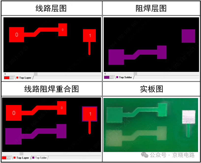
(1) Relationship Between Circuit Layer and Solder Mask Layer: The core of solder mask design lies in understanding the characteristics of its negative output. Simply put, the areas with patterns on the solder mask layer are actually the regions where solder mask ink is not printed, while the areas without patterns will be covered by ink. The areas with patterns on the circuit layer are made of copper, which serves as the path for signal transmission. Only in the areas where the circuit layer and solder mask layer overlap will exposed copper (tin spraying or gold plating) be visible, and these exposed copper areas are used for soldering component pins or for other electrical connections.
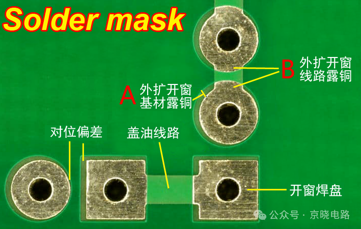
(2) Solder Mask Window and Circuit Pads: Due to alignment deviations in the production process, it is usually required that “the solder mask window pad is larger than the circuit pad” (generally about 0.1mm larger overall, which means an expansion of 0.05mm on each side). However, this may also lead to some issues, such as the solder mask window potentially deforming or enlarging the pad. This is mainly reflected in: when the solder mask window is under an independent circuit pad, the actual pad shape will be consistent with the circuit pad; if it is connected to the circuit pad, the pad will appear larger due to the exposed copper shape of the connected small lines; and for circuit pads on large copper areas, the actual pad shape will resemble the solder mask window pad because the surrounding copper area exposes copper, making the pad appear larger.
Therefore, for special cases where strict requirements are placed on the shape and size of pads, engineers need to design the solder mask size in conjunction with the capabilities of the manufacturer and note not to alter the original solder mask size when placing orders, while carefully checking the production drafts. Currently, some manufacturers have introduced high-end equipment in multilayer board production, which can achieve a 1:1 ratio of solder mask windows to pads. For cases where the solder mask window is too large, the window will be reduced based on the circuit pad to ensure consistency between the two.
Solder Mask Manufacturing Process
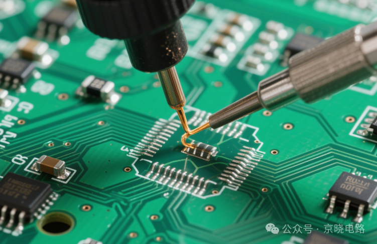
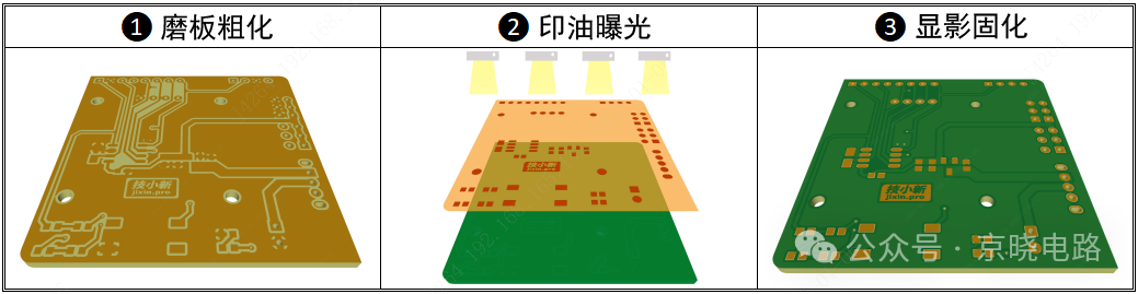
(1) Pre-treatment of Circuit Copper Surface: After completing the drilling, copper plating, and circuit manufacturing processes, the etched circuit copper surface needs to undergo treatments such as board grinding and acid washing. The purpose of this step is to remove oxides and impurities from the board surface while roughening the copper surface to increase the bonding strength between the copper surface and the solder mask ink, preparing for the subsequent solder mask ink printing.
(2) Printing and Exposure: The solder mask ink is evenly printed over the entire board surface and then dried. Next, the solder mask film is placed over the board surface, and ultraviolet light is applied. Under the influence of ultraviolet light, the ink not covered by the solder mask pattern will cure on the board surface and cannot be washed away.
(3) Development Cleaning and Post-processing: After exposure, a development cleaning operation is performed. At this time, the ink covered by the solder mask pattern will be washed away, revealing the original copper surface. These exposed copper areas will undergo tin spraying or gold plating in subsequent processes to meet the requirements for soldering and electrical connections.
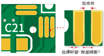
Manufacturing of Solder Mask Bridges
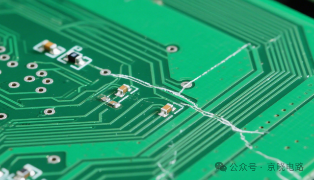
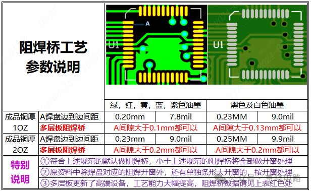
In dense IC pad designs, to reduce the risk of solder flowing to adjacent IC pins during soldering and causing short circuits, solder mask bridges can be designed, which involve printing a layer of solder mask ink between two IC pads. Different colors of solder mask ink and copper thickness have different requirements for the manufacturing of solder mask bridges.
According to Jialichuang PCB ordering, for green, red, yellow, blue, and purple inks, when the finished copper thickness is 10Z, the edge-to-edge spacing of pad A must reach 0.20mm (7.8mil), and the gap for multilayer board solder mask bridges must be greater than 0.1mm; when the finished copper thickness is 20Z, the edge-to-edge spacing of pad A is 0.23mm (9.0mil), and the gap for multilayer board solder mask bridges must be greater than 0.2mm. The requirements for black and white inks will differ. The default for making solder mask bridges is to comply with the above specifications, while those below the specifications will be treated as open windows. If there are large open windows in addition to the solder mask windows corresponding to the pads in the original data, they will also be treated as open windows. With the advancement of technology, manufacturers have introduced high-end equipment in multilayer board production, significantly enhancing process capabilities and optimizing the parameters for solder mask bridge manufacturing.
Conclusion
Solder mask design runs through the entire process of PCB design to production. It is not only a key link to ensure the electrical performance and reliability of PCBs but also an important factor in controlling production costs and enhancing product appearance quality. Whether for electronic engineers, PCB designers, or manufacturing personnel, a deep understanding of the principles and rules of solder mask design is essential to create high-quality PCB products.
END
 Scan to Follow
Focusing on high-speed PCB design, quality assurance
Technical Support: Xiao Jing
 Scan to Follow
Focusing on high-speed PCB design, quality assurance
Jing Xiao Public Account