Previously, I wrote an article on my blog titled “Why Convert PCB Files to GERBER Files and Drill Data for PCB Manufacturers”. That article simply explained why this is necessary. In this article, I will discuss how to convert PCB design files into the corresponding Gerber files and some common pitfalls to avoid.
Many engineers are accustomed to sending their completed PCB files directly to the PCB manufacturer, especially those using Protel, Altium Designer, and PADS, as these file formats are readily accepted by manufacturers. However, these are the source design files, and they ultimately need to be converted into Gerber files by the CAM engineers at the manufacturer. If you provide Gerber files, the manufacturer will directly import them into their CAM system for preprocessing. Many potential PCB production issues often arise from the conversion of Gerber files by the manufacturer’s engineers, especially when dealing with less experienced layout designers who may have non-standard design habits. The CAM engineers at the PCB factory often do not understand PCB design and merely follow the conversion process. If they have questions, they might adjust based on their experience or communicate via phone, but communication between two engineers over the phone can be inefficient, and they might silently criticize each other during the call.

As a result, when the PCB is produced, discrepancies from the design intent may arise, leading to mutual blame and frustration.
I searched for the keyword gerber on a forum of a certain PCB factory and found that there are indeed many misunderstandings regarding the direct submission of PCB design source files through their self-service ordering system.


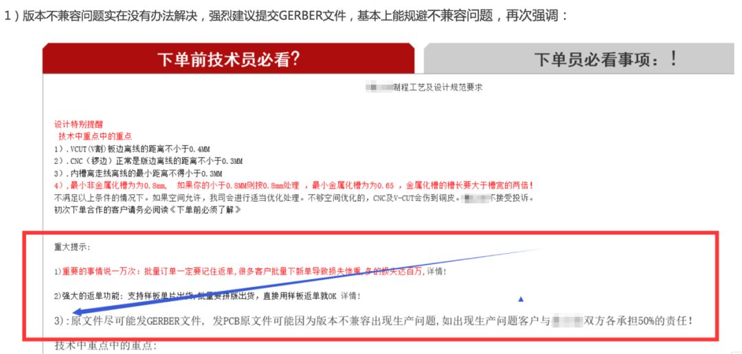
 I strongly agree with this viewpoint: Exporting Gerber files is essential; for every PCB project, convert to Gerber and perform necessary checks (check silkscreen, copper coverage, verify special routing, special pad handling, etc.).
First, let’s explain what Gerber is.
Gerber is a two-dimensional vector image file format. It is the standard format used in PCB industry software to describe the images of printed circuit boards, such as information for the copper layer, solder mask layer, silkscreen layer, drill layer, etc. It serves as an intermediary to convert the graphical data of PCB designs into manufacturing data, essentially a CAD-CAM data conversion format standard.
The Gerber format was originally developed by Gerber Systems Corporation. It is now owned by Ucamco, which acquired Gerber Systems Corporation from Barco.
There are two versions of the Gerber format:
-
Gerber X2: The current latest file format, which is an extension of the RS-274X standard and is backward compatible. It adds previously missing production data, including PCB stack-up structure information, pad and via attributes, and critical impedance-controlled routing information.
-
Extended Gerber format, also known as RS-274X format, is currently widely used.
-
Standard Gerber format, or RS-274D format, has been deprecated and replaced by the RS-274X format.
Note: RS-274D has been deprecated! It has been deprecated! It has been deprecated! Please ensure to use the RS-274X format when exporting Gerber files in the future!!!
One application of the Gerber format is to convert PCB design data from design to production. PCBs are typically designed by PCB designers using specialized Electronic Design Automation (EDA) or Computer-Aided Design (CAD) software, and then output as Gerber format files. The Gerber files are sent to the PCB factory and input into the Computer-Aided Manufacturing (CAM) system to convert the design information, providing data for each process in PCB production.
The safest way to submit PCB production materials to the manufacturer is to export Gerber files yourself, check them in CAM software for accuracy, and then submit the Gerber files along with the manufacturing requirements to the manufacturer.
There is a common misconception that the submitted PCB fabrication files will be used directly for production, with Gerber files going straight to the photoplotter; Excellon drill files going directly to the drilling machine; and IPC-D-356A netlists driving the flying probe test.
However, this is not the case. The manufacturer will not directly use your Gerber files or drill files for production. The primary reason is that PCBs are often produced in panelized form. To reduce manufacturing costs, manufacturers typically panelize smaller boards into larger ones for processing, and then cut them apart in the final manufacturing step. Therefore, manufacturers often combine PCB data from multiple customers onto a single standard panel for production to maximize material usage and reduce costs.
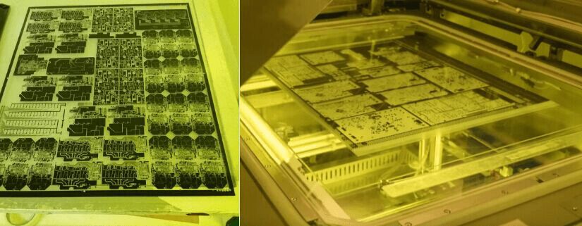 Generally, manufacturers will perform some preliminary processing on the received fabrication files, importing them into CAM software to check if the layer information is complete, if there are any errors, and to confirm the stack-up structure and alignment of the layers. They will also compensate and correct the fabrication files, such as drill compensation, line width and spacing compensation, and analyze the Gerber data to ensure that the design data meets the manufacturer’s process capabilities for smooth production under standard processes.
To be continued…