
Author
Author
Gerry Partida
Vice President of Technology at Summit Interconnect.

PCB companies aim to achieve sustainability goals by reducing waste, conserving energy, and optimizing resources, with sustainability now a primary focus. Discussions about sustainability often center around materials or energy-saving processes, while the core aspect of PCB design is frequently overlooked, despite its central role in manufacturing.
Good design practices, especially those based on established IPC standards, play a crucial role in achieving sustainable PCB production. By ensuring designs are manufacturable and reliable, engineers can significantly reduce the environmental impact of their products. This article will explore how adhering to design rules directly promotes sustainability and why poor design undermines these efforts.
Hidden Costs of Poor Design
Poorly designed PCBs often lead to low manufacturing yields, resulting in higher scrap rates. Whenever a batch of products fails to meet standards, manufacturers must reproduce the circuit boards, consuming additional materials, energy, and labor. This cycle not only increases production costs but also exacerbates the environmental footprint of each PCB.
For example, if the annular ring width in a design is insufficient, or if the spacing between conductors and planes is inadequate, it may lead to defects such as open circuits or short circuits. Poorly conceived or overly complex HDI stack-ups can cause layer alignment issues, delamination, and other non-compliance situations. These problems often require rework or reproduction, both of which are resource-intensive processes. In fact, if a well-structured design that complies with IPC standards were adopted from the outset, the wasted copper, laminates, chemicals, and labor could have been entirely avoided.
Identifying Design Issues: Tools and Missed Opportunities
The industry has developed advanced tools to identify design issues early in the design process, providing opportunities to correct problems before manufacturing begins. PCB design tools such as Siemens NPI (New Product Introduction) and manufacturing tools like Genesis InSight or Integr8tor enable engineers to conduct detailed design rule checks (DRC) and manufacturability analyses. These tools can highlight potential risks in designs, such as misaligned drill files, insufficient copper-to-edge spacing, and poorly optimized stack-ups.
Despite the availability of these tools, many design issues remain unresolved. Faced with flawed designs, many designers choose not to make modifications and instead push the design forward. Such decisions may seem convenient at the moment, but the costs are high: lower manufacturing yields, longer delivery times, and missed delivery commitments.
Moreover, when designers are aware of design issues yet still proceed, sustainability is rarely considered. This decision overlooks the broader environmental impact of increased waste and energy consumption due to rework and overproduction. Every flawed design that enters manufacturing is a missed opportunity—a missed chance to take sustainability seriously and design with long-term efficiency in mind.

The above is an advertisement and is not related to the main content.
One Example of Sustainability Costs: Manufacturing of Glass Fiber Cloth
Glass fiber cloth is a primary component of PCB laminates, providing structural strength, dimensional stability, and critical electrical insulation properties. However, its production process is highly energy and resource-intensive, requiring high precision and specialized skills. The process begins with melting raw materials such as quartz sand, limestone, and other additives in high-temperature furnaces, often exceeding 1700°C. The molten glass is then extruded through fine nozzles to form continuous fibers, which are rapidly cooled to maintain their structural properties. These fibers are gathered into glass bundles and woven into uniform fabric on high-speed looms to meet the stringent requirements of PCB laminates.
After weaving, the glass fiber cloth undergoes cleaning and chemical treatment processes to enhance resin adhesion, ensuring compatibility with the resin systems used in PCB manufacturing. The treated glass fiber cloth is then rolled up, ready to be sent to laminate manufacturers. This process, from raw materials to finished rolls, can take several days and consumes significant energy during heating, cooling, and weaving processes, while also requiring substantial capital investment in advanced equipment. Additionally, the demand for highly skilled operators further increases its costs.
Given the high energy consumption and costs associated with glass fiber cloth production, the environmental impact of waste caused by poor PCB design is magnified. Every additional drilling structure resulting from inefficient design, such as suboptimal stack-ups or overly complex HDI structures, increases the consumption of labor, energy, water, and other materials. Similarly, rework due to design defects exacerbates this waste, squandering the energy and resources already invested in PCB production.
If the electronics industry can address these design inefficiencies, it will take a significant step toward sustainable development. By leveraging advanced design tools and adhering to IPC standards, stack-ups can be optimized to ensure efficient material use, thereby reducing unnecessary demand for glass fiber cloth. Furthermore, utilizing historical data on factory yields and project-specific simulation analyses can help engineers more accurately predict and plan reasonable margins, rather than relying on overly conservative safety margins that double material usage. The environmental and cost benefits of such optimizations are substantial, helping to drive the entire industry toward sustainable manufacturing practices.
Overproduction: A Major Challenge for Sustainability
Another challenge arising from poor design is the demand for overproduction. When a design itself carries the risk of yield loss, manufacturers must produce additional quantities to ensure the required output is met. While this reduces the risk of under-delivery, it comes at the cost of material waste and higher energy consumption.
The issues caused by overproduction extend beyond materials. Each additional PCB produced consumes electricity during imaging, drilling, plating, and testing processes. Even slight overproduction can be magnified in high-volume production, leading to significant environmental impacts.
With modern tools capable of identifying design issues and utilizing historical factory yield data, it is entirely possible to predict expected yields and plan reasonable overproduction accordingly. However, in many cases, the planned level of overproduction remains as high as 100%. When this excessive overproduction is actually executed, it means the industry prioritizes efficiency over sustainability—a choice we can no longer afford.
New Tools for Predicting Sustainability
One of the most promising advancements in sustainable PCB manufacturing is the introduction of tools that can predict the environmental impact of designs. PCB simulation and modeling software company Avishtech recently released a product that can calculate the carbon footprint of PCB designs. This groundbreaking tool can assess design complexity, expected manufacturing yields, and even the environmental impact of the grid used during production. By incorporating these factors, the tool can evaluate the overall sustainability of a design before it enters the manufacturing floor.
This capability represents a disruptive breakthrough for the entire industry. For the first time, engineers can quantify the environmental impact of their design decisions in real-time, allowing for a more informed balance between performance, cost, and sustainability. For instance, if a highly complex design is expected to result in low yields, the tool can highlight the increased carbon footprint due to material waste, energy consumption, and rework. Similarly, the impact of different regional grids—some relying on coal, others primarily on renewable energy—can also be considered, leading to a comprehensive assessment of overall design sustainability.
Figures 1 and 2 provide a comparison of carbon footprints.
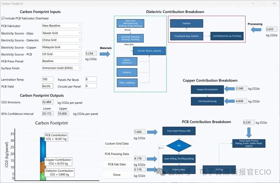
Figure 1: Carbon footprint analysis of a 10-layer design case, which has a relatively low yield and uses materials and processes with a relatively high carbon footprint. This analysis was completed using the Avishtech Gauss Sustainability tool.
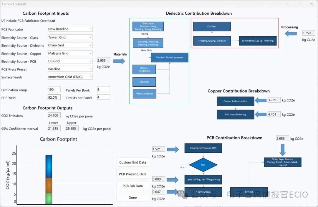
Figure 2: Carbon footprint analysis of the same design case as Figure 1. After optimization to improve yield and using materials and processes with a lower carbon footprint, its carbon footprint was significantly reduced, overall decreasing by approximately 26%.
By providing this level of insight, the tool enables designers to incorporate sustainability into the quantifiable aspects of the design process. This innovation marks a significant step for the PCB industry in aligning with global sustainability goals. It transforms sustainability from an abstract concept into measurable metrics, driving tangible improvements in design practices and manufacturing strategies.
Call to Action for the Industry
As the industry continues to prioritize sustainability, designers will have specific opportunities to drive change. By adhering to good design practices, following IPC standards, and utilizing advanced tools such as carbon footprint predictors, they can create products that perform better while having a smaller environmental footprint.
Manufacturers must also play their part by closely collaborating with design teams to ensure designs are feasible for mass production. Open communication between design and manufacturing teams can identify potential challenges early, reducing the risk of rework and overproduction. Additionally, using tools that emphasize the environmental impact of designs will help manufacturers and designers make sustainability-oriented decisions together.
In PCB manufacturing, sustainability begins with design, but it does not end there. By adopting IPC-compliant design practices, leveraging advanced tools, and fostering collaboration between teams, the PCB industry can reduce waste, conserve resources, and create a greener future for the electronics industry.
END


The above is a partner of the Chief Electronics Officer(partial)
Order does not indicate priority