In the process of PCB design, the segmentation of power planes or ground planes can lead to incomplete planes. When signals are routed, their reference plane may cross from one power plane to another, a phenomenon we refer to as signal cross segmentation.
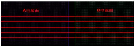
Illustration of cross segmentation phenomenon
Cross segmentation may not have much impact on low-speed signals, but in high-speed digital signal systems, high-speed signals use the reference plane as the return path. When the reference plane is incomplete, the following adverse effects may occur:
a. It can lead to discontinuities in the impedance of the traces;
b. It can easily cause crosstalk between signals;
c. It can trigger reflections between signals;
d. It increases the loop area of the current, increasing loop inductance, making the output waveform prone to oscillation;
e. It increases radiated interference to space and makes it susceptible to external magnetic fields;
f. It increases the possibility of magnetic field coupling with other circuits on the board;
g. The high-frequency voltage drop across the loop inductance forms a common-mode radiation source, which generates common-mode radiation through external cables.
Therefore, PCB routing should be as close to a plane as possible and avoid cross segmentation. If it is necessary to cross segmentation or cannot be close to the power ground plane, these situations are only allowed in low-speed signal lines.
Handling Cross Segmentation in PCB Design
If cross segmentation is unavoidable in PCB design, how should it be handled? In this case, it is necessary to patch the segmentation to provide a shorter return path for the signal. Common methods include adding stitching capacitors and cross-line bridging.
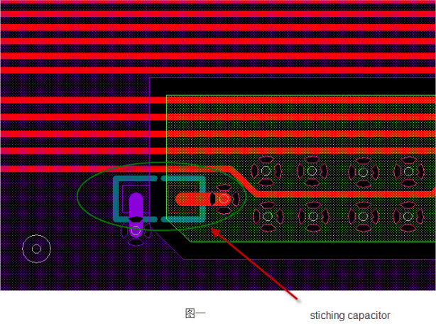
01Stitching Capacitor
Typically, a 0402 or 0603 package ceramic capacitor is placed at the signal cross segmentation point, with a capacitance value of 0.01uF or 0.1uF. If space allows, several such capacitors can be added; at the same time, ensure that the signal line is within 200mil of the stitching capacitor, the closer the better. The networks at both ends of the capacitor correspond to the networks of the reference planes the signal passes through, as shown in the figure below with the networks connected to both ends of the capacitor highlighted in two different colors:
 02Cross-Line Bridging
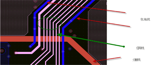
A common method is to perform a “grounding treatment” on the signal that crosses the segmentation on the signal layer, which may also involve grounding other network signal lines. This “grounding” line should be as thick as possible, as shown in the figure below.
 High-Speed Signal Routing Techniques01Multi-Layer Routing
High-speed signal routing circuits often have high integration and density. Using multi-layer boards is not only necessary for routing but also an effective means to reduce interference. Reasonably selecting the number of layers can significantly reduce the size of the printed circuit board, fully utilize the intermediate layers for shielding, achieve better close grounding, effectively reduce parasitic inductance, shorten signal transmission lengths, and greatly reduce cross-interference between signals.
02Minimize Lead Bends
It is best to minimize lead bends between the pins of high-speed circuit devices. The routing of high-speed signal circuits should ideally be straight; if bends are necessary, use 45° angles or arcs. This requirement, which is only used to enhance the adhesion strength of steel foil in low-frequency circuits, can reduce emissions and mutual coupling of high-speed signals in high-frequency circuits, thereby minimizing radiation and reflection of signals.
03Keep Leads Short
It is best to keep leads short between the pins of high-speed signal routing circuits. Longer leads increase distributed inductance and capacitance, significantly affecting the passage of high-frequency signals and altering the circuit’s characteristic impedance, leading to reflections and oscillations in the system.
04Minimize Layer Alternation of Leads
It is best to minimize the alternation of lead layers in high-speed circuit devices. The fewer vias used in the component connection process, the better. Measurements show that one via can introduce about 0.5pF of distributed capacitance, significantly increasing circuit delay. Reducing the number of vias can significantly improve speed.
05Be Aware of Parallel Crosstalk
High-speed signal routing must consider the “crosstalk” introduced by closely parallel signal lines. If parallel distribution cannot be avoided, a large area of “ground” should be arranged on the opposite side of the parallel signal lines to significantly reduce interference.
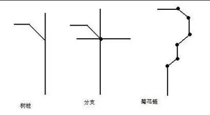
06Avoid Branching and Stubs
High-speed signal routing should avoid branching or forming stubs as much as possible. Stubs have a significant impact on impedance, which can lead to signal reflections and overshoots. Therefore, we typically avoid stubs and branching in design. Using daisy chain routing can reduce the impact on signals.
 07Route Signal Lines on Inner Layers
High-frequency signal lines routed on outer layers are prone to significant electromagnetic radiation and are also easily affected by external electromagnetic radiation or factors. Routing high-frequency signal lines between power and ground lines can reduce radiation significantly through the absorption of electromagnetic waves by the power and bottom layers.
Disclaimer: This article is compiled from the internet, and the copyright belongs to the original author. If there are any copyright issues, please contact us promptly for removal. Thank you!