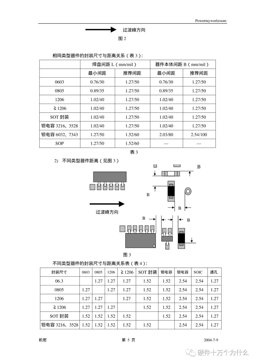
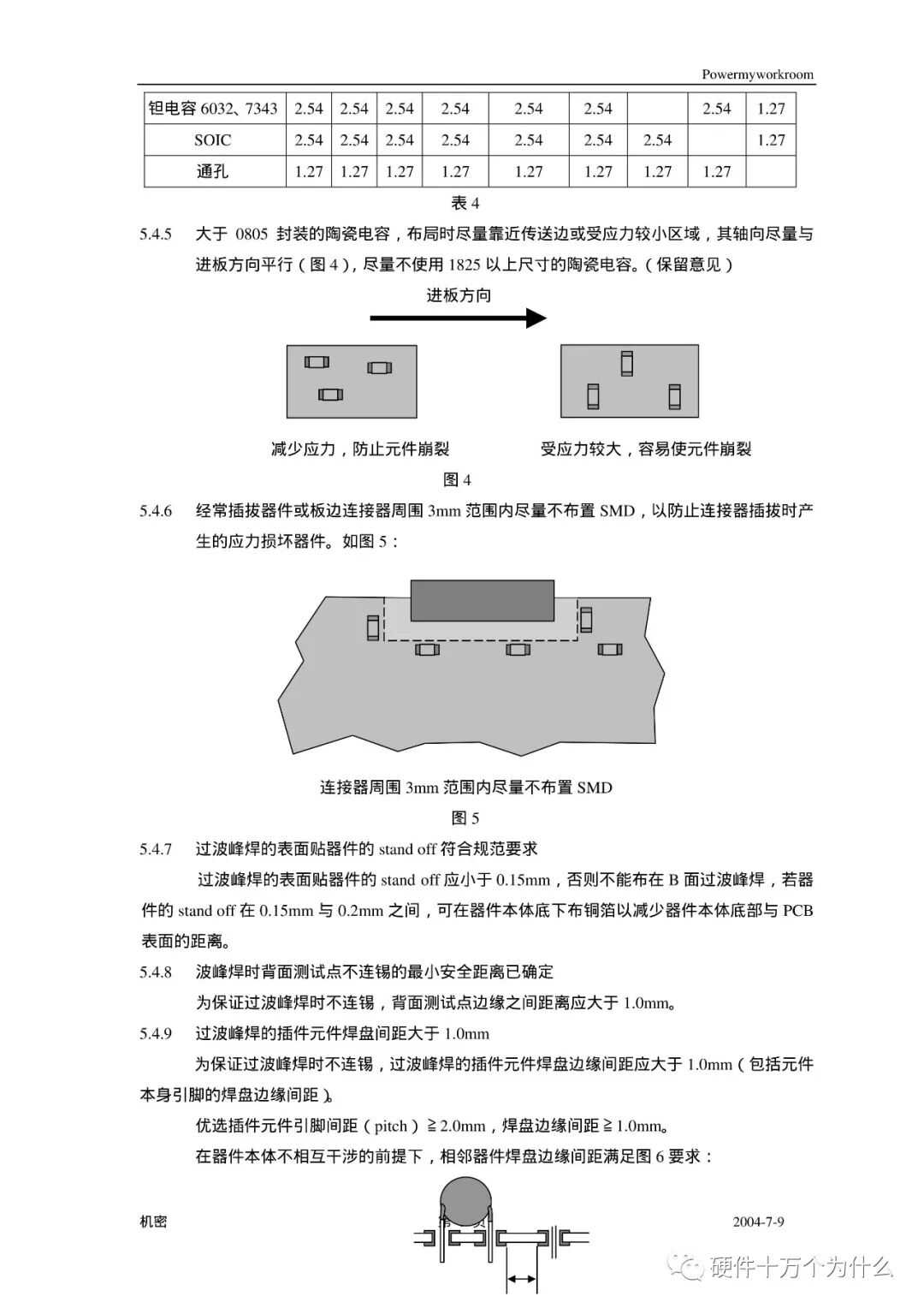
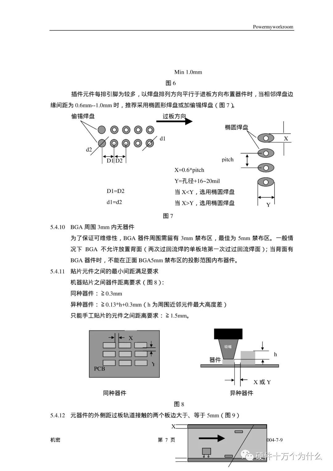
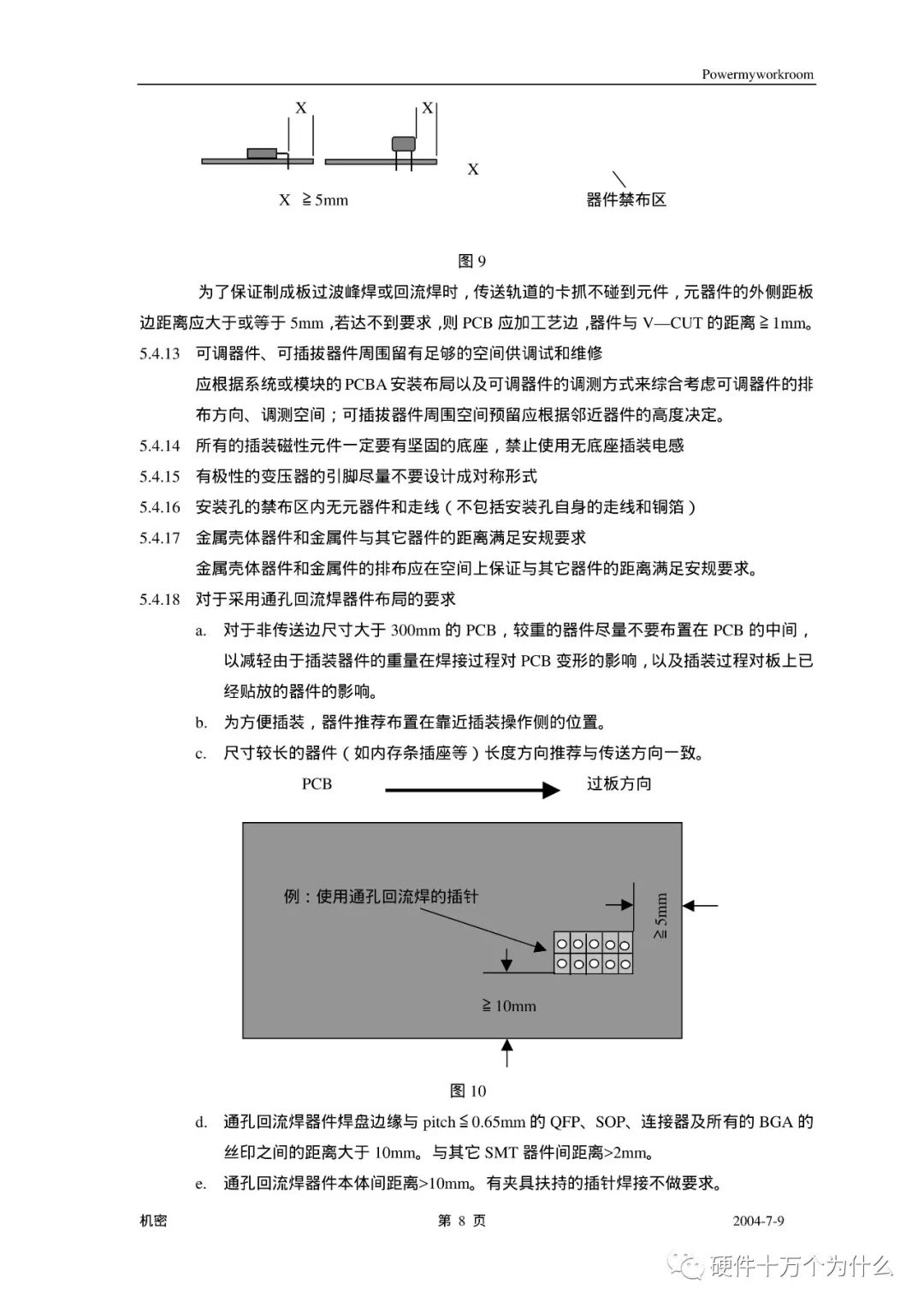
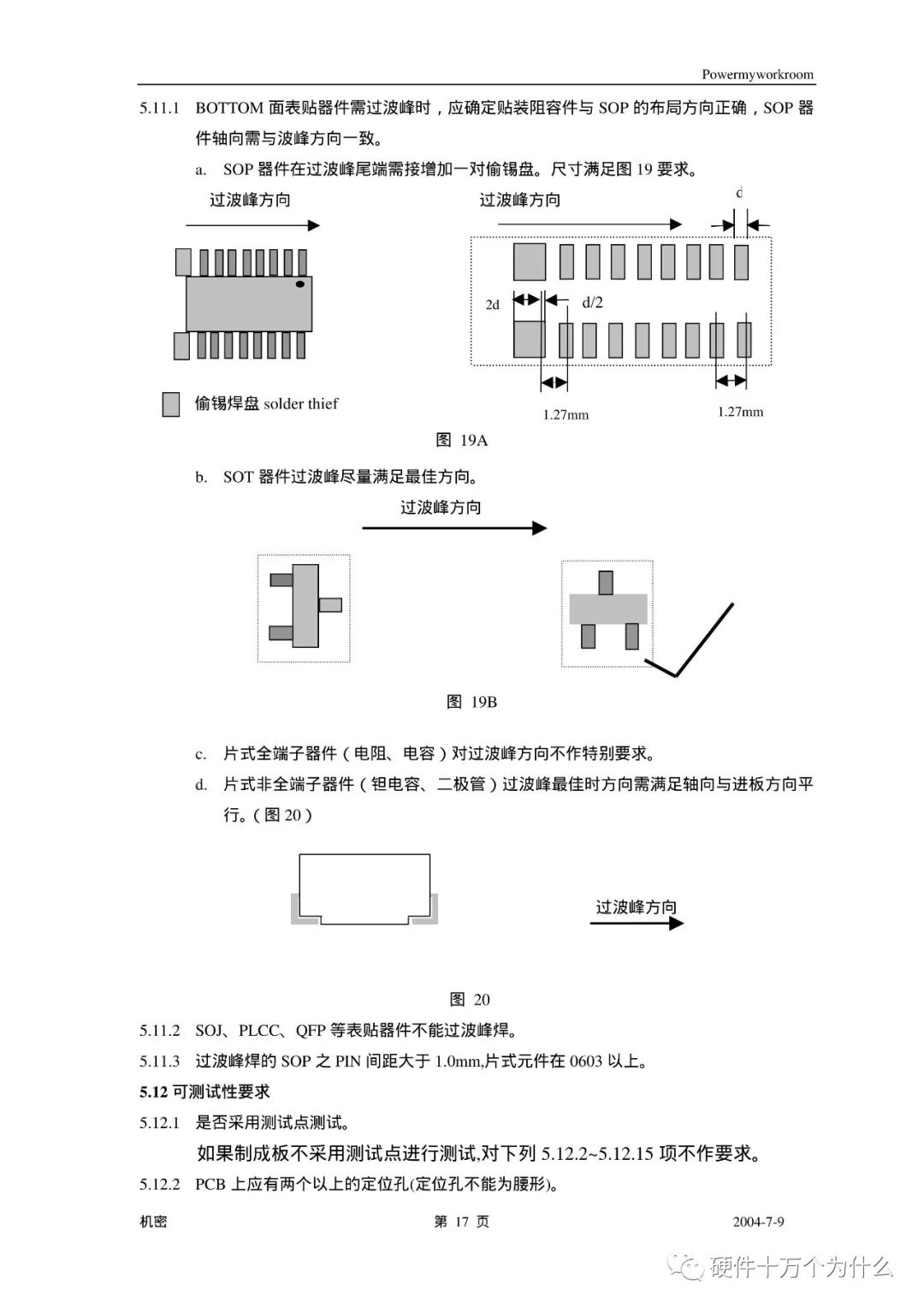
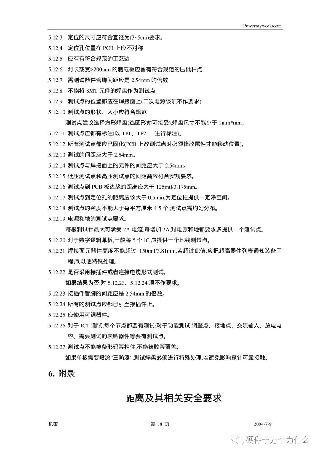
PCB Process Design Specifications Author: Powermyworkroom
Published on: 2004-7-9 (The time is a bit early, but the content is classic)
Related posts
- PCB Factory Owners Cry Out: It’s Too Difficult
- Understanding ADAS Camera Classification and Installation Positions
- High-Speed Communication Between ARM and FPGA
- Overview of VR Devices: Headsets, All-in-Ones, and Mobile
- How to Implement RS-485 Communication for Mitsubishi PLC Control of Mitsubishi Inverters?
- On-Demand Optimizing Deep Learning Model Based on Edge Computing
- Basic Components and Classification of Industrial Robots
- Janus Dual-Atom Catalysts for Electrocatalytic Reactions
- The Amazing Fully Automated Manufacturing Process of a Small SD Card
- 15 Fundamental PLC Concepts for Efficient Learning: How Many Do You Know?
- Download and Installation Guide for Keil uVision 4.22a MDK Version
- Classic! Five AI-Themed Papers from Top Management Journals M&SOM
- 15 PCB Failure Modes and Solutions
- Quantitative Exploration of Faraday’s Electromagnetic Induction Law: Experimental Design and Practical Completion
- Design and Production of Printed Circuit Boards – 460 Pages
- PCB Design Checklist: Routing
- Feasibility Study Report on the Construction Project of PCB Production Base in Pathum Thani, Thailand
- Market Research and Development Trend Forecast Report for the Printed Circuit Board Industry (2025-2031)
- Fundamentals of PCB Design